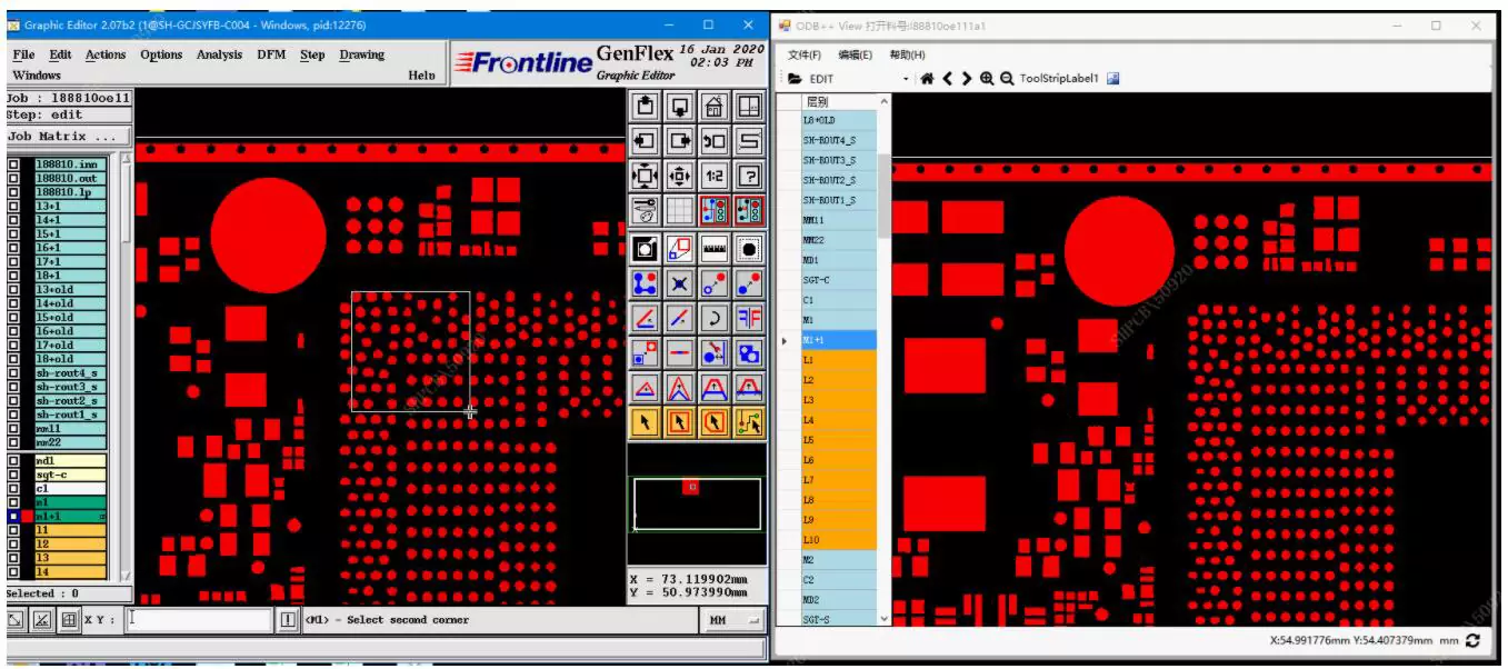
The ODB file is an ASCII-coded, bi-directional transfer file proposed by VALOR (IPC member). The file integrates all functional descriptions of PCB and circuit board assembly. It covers PCB design, manufacturing, and assembly requirements. It includes all PCB drawings, layout layers, layout diagrams, pad stacks, fixtures, and all other information.
The ODB file is mainly proposed to replace the insufficiency of the GEBER file, which contains more manufacturing, assembly information, device information and so on, which is also the manufacturing information we need.
In short, ODB++ file is a kind of manufacturing file which carries more data than GERBER file and less data than PCB manufacturing file.
The ODB++ format was first used by PCB manufacturers. With the ODB++ format, there is no longer a need to collect CAM files in many formats such as Gerber, Excellon, IPC-356 and even IPC-350. The key to the success of the ODB format is that it is recognised by the PCB industry.
CAMCAD can directly read many formats PCB file text format, such as PADS, Protel, P-CAD, etc., but there are also many formats PCB file can not be read directly, then you can through the PCB design software output CAMCAD support for a certain format CAD files and then read, such as ODB + + file. ODB + + is the United States Valor company developed a CAD data format, most PCB design software now supports the output of this format files, such as AD6, MentorExpedition, Cadence, Orcad, Cadstar and so on.
PCB generate ODB++ file. Here we do not generate geber files, or other DXF DWG files, but choose ODB++, ODB++ contains not only component parameters, but also network parameters.
1. Open AD17→file→fabrication output→ODB++ files. In general, double panel, click the bottom plot layers, select ALL OFF, so that only the top_ layer and bottom_ layer will be kept, click OK.
2.The following interface will appear, click OK.
3. Then it will be in the Project Outputs for match_ test_ Project.

PCB design software