1. PCB stencil: definition and basic functions:
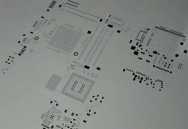
In SMT processes, the PCB stencil is a seemingly simple but crucial component. It is a thin metal plate that has been precisely etched to form holes corresponding to the pads in the PCB design. These holes guide the solder paste during the soldering process, ensuring that the solder paste is accurately deposited onto the designated pad locations on the PCB, which is essential for the subsequent component placement and soldering.
2. There are four production processes for SMT stencil
1. Chemical etching stencil
Features: The stainless stencil sheet is corroded by corrosive chemical solution to obtain the opening corresponding to the PCB pad.
Production process: Cut the steel sheet of appropriate size → Clean → Apply photoresist → UV exposure → Develop and dry → Chemical etching → Strip photoresist → Clean and dry → Check → Stretch → Pack.
2. Laser cutting stencil
Features: High precision, suitable for SMT process with high-density interconnection.
Production process: Data processing → Laser drilling → Grinding, electropolishing → Check → Stretch → Pack.
3. Electroformed stencil
Features: Smooth hole wall, suitable for micro BGA and small chip components.
Production process: Apply photosensitive film on substrate → Make mandrel → Electroplating nickel to generate stencil sheet around mandrel → Stripping and cleaning → Check → Stretch → Pack.
4. Mixed process stencil
Features: It combines the above-mentioned multiple processes to meet the different requirements of different components on the board for the amount of tin.
Production process: Combine one or two of the above three steel mesh processing processes to jointly produce a stencil.
3. Considerations for selecting the process:
1. Determine the most suitable production process according to the type and distribution of components on the board.
2. Consider production efficiency and cost and choose the most suitable production process.
3. For micro BGA and small chip components, electroforming steel mesh is a better choice.
4. For high-precision and high-density SMT processes, laser cutting steel mesh is a better choice.

PCB stencil
4. Files required to make PCB stencil
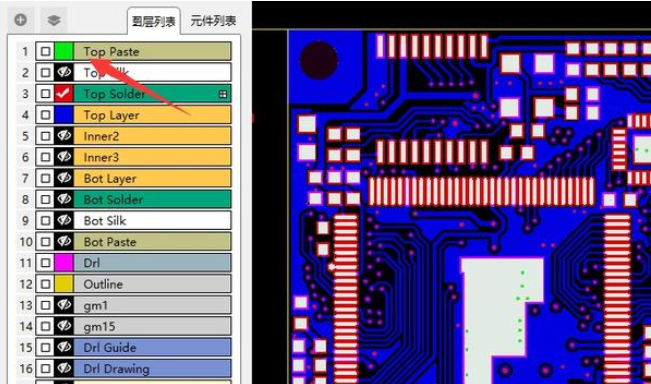
1. Gerber file: This is a standard data exchange format that provides detailed information on various elements on the circuit board, such as line layer, solder mask layer, silkscreenlayer and drilling layer. When making a stencil, at least the SMT layer (GTP and GBP) is required, which is mainly used to define the position and size of the pad.
2. PCB design file: The original PCB file records various information of the PCB board in detail, such as pad position, component layout, etc., providing an accurate reference for the production of the stencil. In addition, you can also use Mechanical 1 as the stencil layer to directly distinguish between patch and plug-in components.
3. Other related files: such as CAD files (such as *.DWG; .DXF) and files generated by specific software (such as .SMD). These files may include brd files (Cadence Allegro, Eagle), max files (Cadence ORCAD), pcbdoc files (Altium Designer), etc., depending on the PCB design software used. These files are used to save and transmit design data.
Together, these files ensure the accuracy and efficiency of stencil production, thereby ensuring the final quality and functionality of the PCB board.

Stencil file
4. How to Choose the Right Stencil
Choosing the right stencil is crucial for ensuring the quality of SMT (Surface-Mount Technology) solder paste printing. When selecting a stencil, several factors need to be considered:
1.Material Selection
Stencils are typically made from stainless steel or other alloys. Different materials have varying hardness, corrosion resistance, and wear resistance. It is important to choose a material that suits the specific application and usage frequency to ensure stable and reliable performance over time.
2.Thickness and Aperture Size
The thickness and aperture size of the stencil directly affect the solder paste printing results. Generally, thinner stencils and smaller apertures provide higher printing precision but may increase the risk of clogging. Therefore, a balance between printing precision and operational stability needs to be found to meet the specific production requirements.
3.Manufacturing Process
The manufacturing process of the stencil impacts its precision and durability. Laser cutting and electrochemical etching are common processes, each with its advantages and disadvantages. The choice of manufacturing process should be based on the specific needs and application scenarios to ensure that the stencil's performance meets expectations.
4.Maintenance and Care
Stencils require regular cleaning and maintenance to remove solder paste residues and contaminants, keeping them in good working condition. Choosing appropriate cleaning agents and maintenance methods can help extend the stencil's lifespan and maintain stable performance.
By considering these factors comprehensively, you can select the most suitable stencil, thereby enhancing the quality and efficiency of SMT solder paste printing.
The PCB stencil is a tool in SMT production that is used to accurately print solder paste onto PCB pads. It is made of a thin metal plate with small holes through which the solder paste flows to achieve precise coating.