Production Requirements for OSP Processing Technology
1.OSP PCB incoming material should be vacuum packed with desiccant and humidity display card. When transporting and storing, use separator paper between PCBs with OSP to prevent friction damage to the OSP surface.
2.OSP PCBs should not be exposed to direct sunlight, maintain a good warehouse storage environment, relative humidity: 30 ~ 70%, temperature: 15 ~ 30 ℃, storage period of less than 6 months.
3.When unpacking OSP PCBs at SMT site,the vacuum packaging must be checked. Drying agent. The unqualified boards should be returned to the manufacturer for rework and reuse, and should be put on the line within 8 hours. Do not unpack more than one package at a time, in accordance with the principle that the number of disassembled that is produced, the number of disassembled production, otherwise the exposure time is too long and prone to batch soldering bad quality accidents.
4.After printing the solder paste as soon as possible after the furnace do not stay (stay up to 1 hour), because the flux inside the solder paste on the OSP film corrosion is very strong.
5.Maintain a good workshop environment: relative humidity 40 ~ 60%, temperature: 18 ~ 27 ℃.
6.Production process to avoid direct hand contact with the PCB surface OSP film, so as to avoid its surface by sweat pollution and oxidation.
7.After the SMT single-side mounting is completed,the second side of the SMT parts must be completed within 12 hours of mounting assembly.
8.After finishing SMT,the DIP insertion should be finished within the shortest possible time (maximum 24 hours).
9.Moisture OSP PCB can not be baked, high temperature baking is easy to make OSP discolouration and deterioration.
10.The overdue empty boards which are not used in production.Moisture empty board.The empty boards after batch printing and cleaning should be returned to the circuit board manufacturer for OSP processing, but the same board can not be used for more than three times of OSP processing,otherwise,it needs to be scrapped and disposed of.

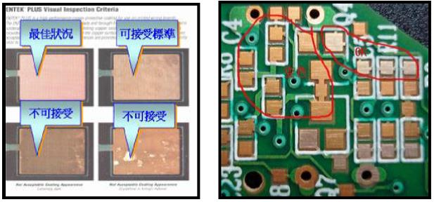
Acceptable standard reference for OSP PCB pad discoloration
OSP PCB SMT solder paste stencil design requirements
1.OSP because of the flat, favourable to paste forming, and PAD can not provide a part of the solder, so the opening should be appropriately enlarged to ensure that the solder can cover the entire pad.When the PCB is changed from OSP to OSP, the stencil has to be reopened.
2.After the opening is appropriately enlarged, in order to solve the problem of SMT CHIP pieces of tin beads.After the opening is appropriately enlarged, in order to solve the problem of tin beads on SMT CHIP parts, and the problem of exposed copper on OSP PCBs, we can change the design of the stencil opening for solder paste printing into a concave design, with special attention to the prevention of tin beads.
3.If there are no parts placed on the PCB for any reason, the solder paste should cover the pads as much as possible.
4.In order to prevent oxidation of the exposed copper foil, which may cause reliability problems, it is necessary to consider the ICT test point.Installation screw holes.In order to prevent oxidation of the exposed copper foil, it is necessary to consider printing solder paste on the front side of the ICT test points, mounting screw holes, exposed through holes, etc.(wave soldering on the reverse side), and to give full consideration to opening the holes when making the stencil.
Requirements for handling defective OSP PCB printed solder paste boards
1.Avoid printing errors as much as possible, because cleaning will damage the OSP protective layer.
2.When the PCB printing solder paste is bad, because the OSP protective film is very easy to be eroded by organic solvents, all OSP PCBs should not be soaked or cleaned with high volatile solvents, and can be wiped off with a non-woven cloth moistened with 75% alcohol, and then blown dry in a timely manner with an air gun.Do not use isopropyl alcohol (IPA) to clean, must not use a mixing knife to scrape off the solder paste on the poorly printed board.
3.After the PCB is cleaned up, the SMT soldering of the PCB should be completed within 1 hour.
4.If there is a batch (e.g.20PCS and above) of printing defects, we can take a centralised return to the factory heavy pipeline processing.
OSP PCB reflow oven temperature curve setting requirements
OSP PCB reflow soldering temperature curve setting requirements and tin spray board is basically the same, the maximum peak temperature can be appropriately adjusted down 2-5 ℃.
OSP Processing Technology Introduction: OSP is the abbreviation of Organic Solderability Preservatives, meaning: Organic Protective Film, also known as Copper Protectant.It is a process of coating a layer of OSP film (usually controlled at 0.2-0.5um) on bare copper solder pads (double-sided/multi-layer/two-layer) for protection, replacing the original surface of the pads with a process of spraying tin and other protective treatments.
Advantages of OSP technology: low PCB production cost.High surface flatness of the pad to meet the requirements of lead-free technology.
Disadvantages of OSP process: High requirement for use (limited use after opening.Limited time to complete the front and back side.The insert wave soldering production), high storage environment requirements, OSP surface is easy to oxidise, moisture usually can't be baked and reused, poorly printed PCB can't be cleaned and reused casually.