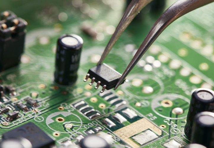
PCB surface finish is a process to form a protective layer on the solderable area to guarantee good solderability and electrical properties. The surface finish prevents oxidization of the copper surface, improves soldering quality, and extends the life of the PCB.

FR-4 PCBs' surface finish
1. Organic protective film (OSP): the use of chemical coating layer of organic materials, to protect the pads and vias, simple and low-cost process, but the film thickness is thin, and easy to operate due to poor solderability.
2. Hot air leveling (HASL): the molten solder coated on the surface of the PCB Circuit Board, and then leveled with hot air. The process is mature, and low cost, but will form a turtle back phenomenon
on the pad, affecting the surface flatness.
The Hot Air Solder Leveling (HASL) process is a crucial step in Printed Circuit Board (PCB) manufacturing, ensuring a flat and uniform solder coating on copper surfaces.
This process involves several stages, beginning with dip soldering where the board is immersed in molten solder to coat the exposed copper. This initial coating provides a base for the subsequent leveling.
Following the initial solder application, the PCB undergoes hot air leveling. This stage involves using high-pressure hot air nozzles, typically at around 250°C, to remove excess solder. The precise temperature and pressure are critical to shape the molten solder into a uniform thickness without damaging the pads or solder mask. After leveling, the board is rapidly cooled to solidify the solder, forming robust solder joints. This quick cooling prevents uneven layers and ensures the integrity of the solder.
Finally, a post-cleaning phase removes any solder or flux residues, which is essential for subsequent component mounting and overall reliability. The boards then undergo a thorough quality inspection, including visual checks for defects like tin bridges or voids, and thickness measurements using equipment such as XRF to ensure compliance with IPC standards. Qualified PCBs are then packaged to prevent moisture and oxidation before storage or shipment.
3. Immersion Tin: the same tin replacement of copper to form a protective layer, with good solderability. However, the storage time is short and prone to the phenomenon of tin whiskers.
4. Immersed silver: through the replacement of copper deposited silver layer, the process is relatively simple, good solderability. However, it is easy to oxidize, resulting in appearance and solderability problems.
5. Immersion gold (ENIG): chemical methods in the PCB conductor deposition of nickel, and then deposited on the gold layer. It has good pad flatness and protection, but the process is complex and costly.
6. ENEPIG: through chemical methods on the surface of the copper layer plated with a layer of nickel, palladium, and gold, nickel palladium gold surface treatment because of
its good electrical and antioxidant properties, can be used for gold wire bonding.
7. Gold plating: It is divided into hard gold plating and soft gold plating. Hard gold plating is technically known as hard electrolytic gold and usually consists of 99.6% or 99.9% pure gold. These gold particles are attached to the PCB surface through electroplating. The structure of hard gold makes it more wear-resistant and therefore suitable for frequently touched components such as connectors and pushbutton PADs. Soft gold plating refers to the plating of a softer layer of gold on top of a nickel coating on the PCB surface. Typically, soft gold plating has a higher purity gold layer (typically 99.9%).
8. Silver plating: the use of chemical or electroplating technology in the metal surface plated with a layer of silver, the silver-plated layer has a high degree of electrical conductivity and good light reflection ability, but the main problem is that the silver layer is easy to oxidize, after a long period after the use of the silver layer may turn black, thus affecting the appearanceand performance.
9. Tin plating: The tin plating process is generally divided into two kinds electroplating and chemical plating. Electroplated tin is usually deposited on the metal surface by electrolysis, while chemical tin plating relies on chemical reactions. Electroplating is faster, and chemical plating is capable of achieving uniform coatings on complex-shaped workpieces.
Choosing the right PCB surface finish process can meet the specific needs of different products in terms of durability, appearance, and performance, and enhance the performance of the product.