The design of high speed PCB vias is actually very particular. Today, I will share with you the technical knowledge of vias and back drilling in PCBs.
Via design in high-speed PCBs In high-speed PCB design, multi-layer PCBs are often required, and vias are an important factor in multi-layer PCB design.
2.The vias in PCBs are mainly composed of three parts: holes, pad areas around holes, and POWER layer isolation areas.

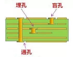
Via Type
1. The impact of vias in high-speed PCBs In high-speed PCB multi-layer boards, signals need to be connected through vias when they are transmitted from one layer of interconnection lines to another layer of interconnection lines. When the frequency is lower than 1GHz, vias can play a good connection role, and their parasitic capacitance and inductance can be ignored.
When the frequency is higher than 1 GHz, the parasitic effect of vias cannot be ignored in terms of signal integrity. At this time, vias appear as discontinuous impedance breakpoints on the transmission path, which will cause signal reflection, delay, attenuation and other signal integrity problems.
When the signal is transmitted to another layer through a via, the reference layer of the signal line also serves as the return path of the via signal, and the return current will flow between the reference layers through capacitive coupling and cause problems such as ground bounce.
2. Types of vias Vias are generally divided into three categories: through holes, blind holes and buried holes. Blind holes: refer to holes located on the top and bottom surfaces of a printed circuit board, with a certain depth, used to connect the surface circuit and the inner layer circuit below. The depth of the hole and the hole diameter usually do not exceed a certain ratio.
Buried holes: refer to connection holes located on the inner layer of a printed circuit board, which do not extend to the surface of the circuit board.
Through holes: This type of hole passes through the entire circuit board and can be used to achieve internal interconnection or as a component installation positioning hole. Because through holes are easier to implement in terms of process and have lower costs, they are generally used in printed circuit boards.
3. Via design in high speed PCB In high-speed PCB design, seemingly simple vias often have a great negative effect on circuit design. In order to reduce the adverse effects of the parasitic effects of vias, the following can be done as much as possible in the design:
(1) Choose a reasonable via size. For multi-layer PCB designs with normal density, it is better to use vias of 0.25mm/0.51mm/0.91mm (drilling/pad/POWER isolation area); for some high-density PCBs, 0.20mm/0.46mm/0.86mm vias can also be used, and non-through holes can also be tried; for vias of power or ground wires, larger sizes can be considered to reduce impedance;
(2) The larger the POWER isolation area, the better, considering the via density on the PCB, generally D1=D2+0.41;
(3) The signal traces on the PCB should not change layers as much as possible, that is, minimize the number of vias;
(4) Using a thinner PCB is conducive to reducing the two parasitic parameters of vias;
(5) The power and ground pins should be close to the vias, and the leads between the vias and the pins should be as short as possible, because they will increase the inductance. At the same time, the power and ground leads should be as thick as possible to reduce impedance;
(6) Place some ground vias near the vias where the signal changes layers to provide a short-distance loop for the signal. In addition, the via length is also one of the main factors affecting the via inductance. For vias used for top and bottom layer conduction, the via length is equal to the PCB thickness. Due to the increasing number of PCB layers, the PCB thickness often reaches more than 5 mm. However, in high-speed PCB design, in order to reduce the problems caused by vias, the via length is generally controlled within 2.0 mm. For vias with a length greater than 2.0 mm, the impedance continuity of the via can be improved to a certain extent by increasing the via diameter. When the via length is 1.0 mm or less, the optimal via diameter is 0.20 mm ~ 0.30 mm.

2. Back drilling process in PCB board production
1. What is PCB back drilling? Back drilling is actually a special type of deep hole drilling. In the production of multi-layer boards, such as 12-layer boards, we need to connect the 1st layer to the 9th layer. Usually we drill a through hole (one-time drilling) and then deposit copper. In this way, the 1st layer is directly connected to the 12th layer. In fact, we only need to connect the 1st layer to the 9th layer. The 10th to 12th layers are like a pillar because there is no line connecting them. This pillar affects the signal path and causes signal integrity problems in communication signals. Therefore, this extra pillar (called STUB in the industry) is drilled out from the back (secondary drilling). So it is called back drilling, but it is generally not drilled so cleanly, because the subsequent process will electrolyze a little copper, and the drill tip itself is also sharp. Therefore, PCB manufacturers will leave a small point. The length of this STUB left is called the B value, which is generally in the range of 50-150UM.
2. What are the advantages of back drilling?
1) Reduce noise interference;
2) Improve signal integrity;
3) Reduce local board thickness;
4) Reduce the use of buried and blind holes, and reduce the difficulty of PCB board production.
3. What is the role of back drilling? The role of back drilling is to drill out the through-hole sections that do not play any connection or transmission role, so as to avoid reflection, scattering, delay, etc. of high-speed signal transmission, which will bring "distortion" to the signal. Research shows that the main factors affecting the signal integrity of the signal system are design, board materials, transmission lines, connectors, chip packaging and other factors. The conductive hole has a greater impact on signal integrity.
4. The working principle of back drilling production relies on the micro-current generated when the drill needle touches the copper foil on the substrate surface when drilling, to sense the height position of the board surface, and then drill according to the set drilling depth, and stop drilling when the drilling depth is reached. As shown in Figure 2:
5. What is the process flow of back drilling?
a. Provide a PCB with positioning holes on it, and use the positioning holes to position the PCB and drill holes;
b. Electroplate the PCB after drilling, and seal the positioning holes with dry film before electroplating;
c. Make an outer layer pattern on the electroplated PCB;
d. Electroplate the pattern on the PCB after the outer layer pattern is formed, and seal the positioning holes with dry film before electroplating;
e. Use the positioning holes used by a drill to perform back drilling positioning, and use a drill to back drill the electroplated holes that need to be back drilled;
f. Wash the back drilled holes with water after back drilling to remove the drill chips remaining in the back drilled holes.
6. What are the technical features of back drilled boards?
1) Most backplanes are hard boards
2) The number of layers is generally 8 to 50
3) Board thickness: 2.5mm or more
4) Thickness-diameter ratio is relatively large
5) Board size is relatively large
6) Generally, the minimum hole diameter for the first drill is >= 0.3mm
7) There are fewer outer layer lines, and most of them are designed as crimp holes
8) The back drilled holes are usually 0.2MM larger than the holes that need to be drilled
9) Back drill depth tolerance: +/-0.05MM
10) If the back drill is required to drill to the M layer, the dielectric thickness from the M layer to the M-1 layer (the next layer of the M layer) is at least 0.17MM.
7. What fields are back drilled pcb boards mainly used in?
Backplanes are mainly used in communication equipment, large servers, medical electronics, military, aerospace and other fields. Since military and aerospace are sensitive industries, domestic backplanes are usually provided by military and aerospace system research institutes, R&D centers or high speed PCB manufacturers with strong military and aerospace backgrounds; in China, the demand for backplanes mainly comes from the communication industry, and the communication equipment manufacturing field is now gradually growing.