The pcb silkscreen layer of a PCB is a text layer, which is generally used for annotations. Its function is to facilitate the installation and maintenance of circuits. The silkscreen layer usually has a top silkscreen layer (Top Overlay) and a bottom silkscreen layer (Bottom Overlay), both of which are used to mark the projection outline of components, component numbers, nominal values or models, and various annotation characters.
So, what are the factors that affect PCB silkscreen?
1. Placement position
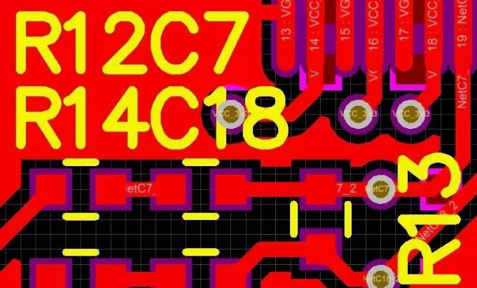
Generally speaking, when placing the PCB silkscreen of components such as resistors, capacitors, and tubes, do not use four directions. This will make it very tiring to read the silkscreen during debugging, maintenance, and welding (the board needs to be turned in several directions).
Therefore, it is recommended to place it in two directions, as shown in the figure below. In this way, it will be very convenient to check the silkscreen. If the components are too dense and the silkscreen cannot be placed, you can write the silkscreen in the blank space nearby, mark the arrow, and it is best to draw a frame, so that it is easier to identify.

PCB silkscreen
2. The reading direction of the pcb silkscreen should be consistent with the direction of use, and the pin number should be clearly marked
The reading direction of the silkscreen should be consistent with the direction of use of the chip, mainly to reduce the probability of reverse welding during welding.
Others, such as electrolytic capacitors, etc., can also not follow this suggestion, because you can mark the positive and negative polarity.
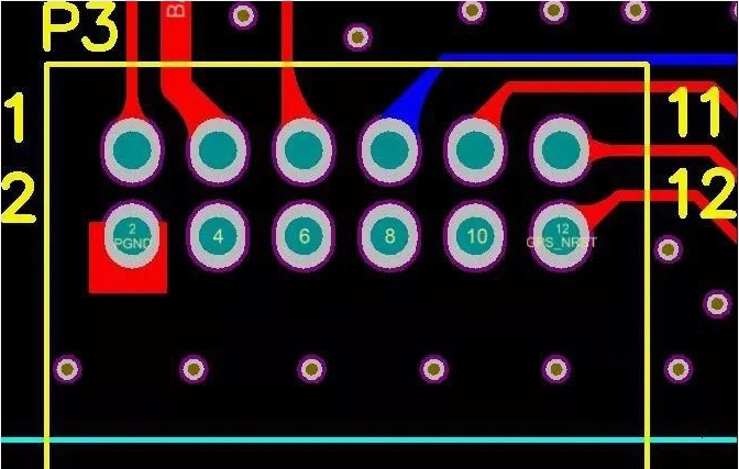
As shown in the figure below, 4 pin numbers are marked on the P3 connector for easy debugging/installation. In addition, it is best to mark the pins in densely populated areas, such as chips, FPC sockets, etc.
At the same time, it also meets the previous suggestion that the reading direction of P3 is consistent with the direction of use of the connector.

3. PCB Silkscreenof special packages and silk screen of mounting holes
For special packages such as BGA and QFN, the size of the silk screen should be exactly the same as the size of the chip (as shown in the figure below), otherwise, it will be difficult to align, thus affecting welding.

4. Ambiguity of silkscreen printing: Functions need to be indicated separately
Many people will mark RX and TX for the commonly used RS232, but there are also RX and TX on the PC side. When should cross lines be used and when should non-cross lines be used?
This leads to ambiguity in PCB silkscreen printing, which makes it difficult to distinguish.
Two arrows are added here to indicate the direction of the signal flow (as shown in the figure below), so that you can know how to connect at a glance.
This can be done not only for RS232, but also for other devices with transmit and receive signal lines, such as SPI, etc.