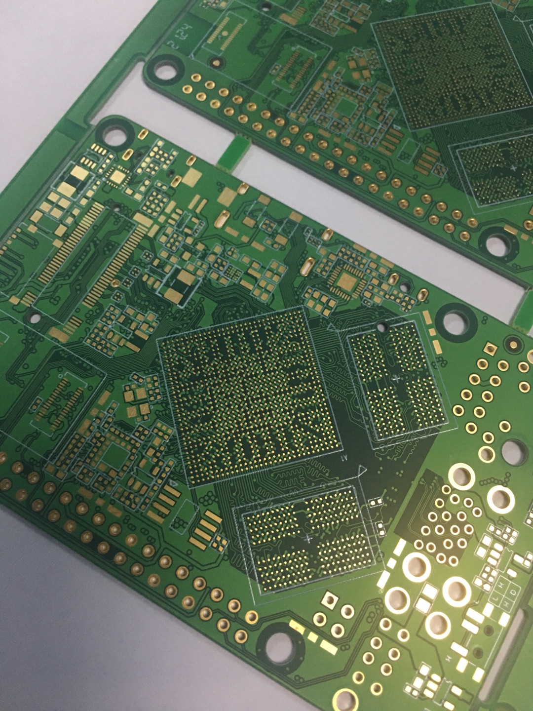
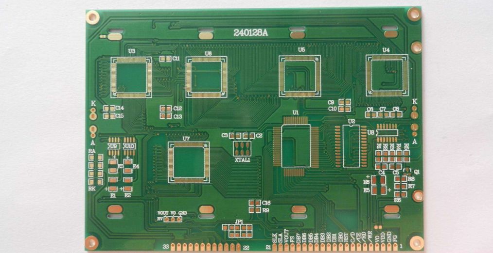
A HDI board is a circuit board manufactured using high-density micro-wiring and micro-via technology. A high-density interconnect (HDI) board (HDI) is a circuit board with a relatively high wiring density, using micro-blind and buried via technology. HDI boards have inner and outer layers of wiring, and processes such as drilling and in-hole metallization are used to connect the wiring within each layer.
HDI boards are generally manufactured using a build-up method. The higher the number of build-ups, the higher the technical level of the board. Ordinary HDI boards typically have a single build-up, while high-end HDI boards use two or more build-ups, employing advanced PCB technologies such as stacked vias, electroplated via filling, and laser direct drilling. When PCB density exceeds eight layers, HDI manufacturing can be more cost-effective than traditional, complex press-fit processes.

HDI boards
HDI boards facilitate the use of advanced packaging technologies, and their electrical performance and signal accuracy are superior to traditional PCBs. Furthermore, HDI boards offer improved resistance to radio frequency interference (RFI), electromagnetic interference (EMI), electrostatic discharge (ESD), and thermal conductivity. Electronic products are continuously evolving toward higher density and higher precision. This "high" not only improves performance but also reduces size. High-density integration (HDI) technology enables even more compact end-product designs while meeting higher standards for electronic performance and efficiency. Many popular electronic products, such as mobile phones, digital cameras, laptops, and automotive electronics, utilize HDI boards.
With the continued evolution of electronic products and market demand, HDI boards are poised for rapid growth. Due to the influence of drill bits, drilling holes in traditional PCBs becomes prohibitively expensive once the hole diameter reaches 0.15mm, and further improvement is difficult. HDI boards no longer rely on traditional mechanical drilling, but instead utilize laser drilling technology (hence, sometimes called laser boards). HDI board holes typically have a diameter of 3-6 mils (0.076-0.152mm), and trace widths are typically 3-4 mils (0.076-0.10mm). This significantly reduces pad size, allowing for more traces per unit area, resulting in high-density interconnects. The emergence of HDI technology has adapted to and advanced the development of the PCB industry, enabling denser arrangements of BGAs, QFPs, and other components within HDI boards.
Advantages of HDI Boards
1. Increased Circuit Density
Traditionally, interconnects between PCBs and components must be made via traces and through-hole conductors extending from the periphery of the QFP (fan-in and fan-out methods), requiring considerable space.
Microvia technology, however, allows interconnection wiring to be hidden on the next layer. The connection between pads and leads on different layers is achieved directly through blind vias within the pads, eliminating the need for fan-in and fan-out wiring. Therefore, solder pads (such as mini-BGA or CSP solder balls) can be placed on the outer layers to accommodate more components, increasing the density of the circuit board.
HDI boards also feature smaller hole diameters and pads, saving space and increasing wiring density.
Many high-function mobile phone boards currently utilize this new wiring method.
2. Light, Thin, Short, and Small
The increased wiring density allows PCBs to accommodate more wiring within a smaller space, achieving the required functionality. This reduces the PCB area. Furthermore, fewer layers are required to achieve the same functionality, reducing the overall thickness of the PCB.
3. Facilitates the use of advanced assembly technologies
Traditional drilling techniques, due to issues with pad size (through-holes) and mechanical drilling, cannot meet the requirements for small components with fine circuits.
Utilizing process advances in microvia technology, designers can incorporate the latest high-density IC assembly technologies, such as matrix packaging (MA), CSP, and DCA (Direct Chip Attach), into their systems.
4. Better electrical performance and signal accuracy
Microvia interconnects not only reduce signal reflections and crosstalk between circuits, but also allow for more space in circuit board designs. Due to their small, short physical structure, microvias can reduce inductance and capacitance, and also reduce switching noise during signal transmission.
5. Better reliability
Due to their thinner thickness and 1:1 aspect ratio, microvias offer higher signal transmission reliability than standard through-holes.
6. Improved thermal properties
HDI boards' insulating dielectric material has a higher glass transition temperature (Tg), resulting in better thermal properties.
7. Improved radio frequency interference, electromagnetic interference, and electrostatic discharge (RFI/EMI/ESD)
Microvia technology allows PCB designers to shorten the distance between the ground layer and the signal layer, reducing radio frequency interference and electromagnetic interference. Furthermore, it can increase the number of ground lines, preventing damage to circuit components caused by static electricity buildup and resulting in instantaneous discharge. 8. Increased Design Efficiency
Microvia technology allows circuits to be placed on inner layers, giving circuit designers more design space and thus improving circuit design efficiency.
HDI Board Design Considerations
1. Laser hole diameter: 0.076-0.15mm (3-6 mil); ring width: ≥3 mil;
2. Laser holes cannot be drilled through, and dielectric thickness must be ≤0.1mm;
3. Copper thickness of laser hole processing layers and laser hole connection layers must be ≤1oz;
4. The stackup design must be symmetrical. The number of completed board layers must be even, and the copper and dielectric thicknesses of each layer must be as symmetrical as possible.

HDI boards
Differences between HDI Boards and Ordinary PCBs
Introduction to Ordinary PCBs: PCBs (Printed Circuit Boards), also known as printed circuit boards in Chinese, are important electronic components that support electronic components and provide the electrical connections for them. Because they are produced using electronic printing technology, they are called "printed" circuit boards. Its primary function is to ensure that electronic devices employ printed circuit boards (PCBs). The consistency of similar PCBs prevents manual wiring errors. It also enables automated insertion and placement of electronic components, automated soldering, and automated testing, ensuring the quality of electronic devices, improving productivity, reducing costs, and facilitating repairs. The difference between HDI boards and ordinary PCBs: Ordinary PCBs are primarily made of FR-4, a laminate of epoxy resin and electronic-grade glass cloth. Traditional HDI boards typically use adhesive-backed copper foil on the outermost layer. Because laser drilling cannot penetrate the glass cloth, adhesive-backed copper foil without fiberglass is typically used. However, today's high-energy laser drills can penetrate 1180 glass cloth, making them indistinguishable from ordinary materials.