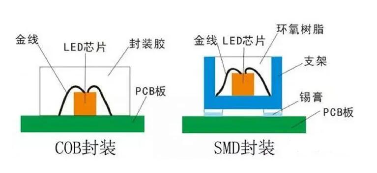
COB packaging, known as Chips on Board (COB), is a technology that solves the problem of heat dissipation in LEDs. The COB process involves bonding the bare chip to the interconnecting substrate with conductive or non-conductive adhesive, and then bonding the wires to realise the electrical connection.
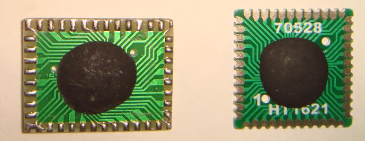
Careful friends may find that there are some PCB boards or black packaging things. So what is this thing? Why are they on the PCB? In the end, what is the important role? In fact, it is used as a kind of packaging. We can often call it COB packaging.

Features of COB process
1.COB packaging is fully known as chip-on-board packaging, is the solution to the problem of LED heat dissipation technology. Compared with inline and SMD, it features space-saving, simplified packaging work, and efficient thermal management pipeline.
2.COB packaging is the bare chip with conductive or non-conductive adhesive adhesive on the interconnecting substrate, and then lead bonding to achieve their electrical connection.
3.When the bare chip is directly exposed to the air, it is easy to be contaminated or man-made damage to affect or destroy the function of the chip, and encapsulate the chip and bonding leads to solve the problem. This is also known as soft encapsulation.
This is the bonding process in the COB wafer manufacturing process. It is called chip on board, i.e. chip package on board. COB process is one of the bare chip mounting technologies. Epoxy resins are used to bond chips on PCBs. So why do some PCBs not have this type of packaging and what are the characteristics of this type of packaging?
Sometimes we actually don't want to add cost. COB packaging process as the simplest bare chip mounting, in order to protect the circuit internal IC from damage, this packaging can generally require a one-time molding, generally placed on the circuit board on the surface of the copper foil, the shape is round, the colour is black. COB packaging if the bare chip is directly exposed to the air, vulnerable to contamination or human damage, affecting or destroying the chip function, so the chip and bonding leads with glue to seal up. This is also known as a soft package.
The COB packaging process has low cost, space-saving optical and thermal effects, and a simple packaging method. In particular, it is the most cost effective for integrated circuits. This method is only related to the multiple leads of the IC chip. The COB package process manufacturer then deposits the adhesive on the circuit board, has a good soldering machine, and then cures the adhesive to make it hard.

Advantages of COB process
1.COB packaging process of better protection
Ordinary LED display in the transport or installation process, if subjected to greater external forces, may cause individual lamp beads or welding off, then it will cause some points of bad points, not light, monochrome display and other phenomena, which is very much related to the packaging process. The introduction of COB packaging, to a large extent, to improve this phenomenon, because the COB packaging is directly to the LED chip packaging in the PCB board of the concave light groove, and then fixed with epoxy resin, so the entire lamp ball is a raised sphere, the overall smooth and hard, so better protection performance.
2.COB packaging process point spacing is smaller
COB packaging process can be done to reduce the LED lamp beads point spacing, the original SMD packaging of the LED display screen point spacing can only do P1.3 or so, and then further down it is difficult to achieve and can not guarantee a certain range of dead lights, and COB packaging changes the arrangement of LED lamp beads and the composition of the pipeline, so in essence, it can be done to achieve a smaller point spacing, such as P2, P0.9, and other types of models.
3.COB packaging process less bad lights, long life
As the COB packaging technology products are packaged in the light on the PCB board, through the copper foil on the PCB board to quickly transmit the heat of the lamp core, and the thickness of the copper foil on the PCB board have stringent process requirements, coupled with the fine craftsmanship, will not cause excessive light attenuation, so very few bad lights, and greatly extends the service life of the LED display screen.
Disadvantages of COB process
1.COB packaging process production difficulties
LED display in COB packaging, to ensure that each lamp is no problem before the glue, unlike SMD packaging can be individually replaced by a lamp bead, for the entire packaging process requirements are very high, so it is difficult to produce, and at the same time it is also much higher prices.
2.Inconvenient maintenance of COB packaging process
For the traditional SMD packaging, LED display if there is a bad light, you can disassemble the unit board after the welding of a single lamp bead can be repaired, and COB packaging products if the maintenance will affect the surrounding lights, so the maintenance difficulty is relatively high. Although COB package has better protection performance, but there will be a certain amount of bad lights, but the failure rate is lower, and in this case can only replace a unit of PCB board.