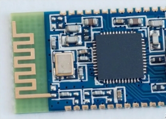
What is PCB Edge Plating?PCB edge plating,also known as edge coating, is the copper plating that extends from the top to the bottom surface of the board, covering at least one peripheral edge. PCB edge plating strengthens the connection of the PCB and reduces the likelihood of device failure. It is particularly common in small PCBs and motherboards, with examples often found in Wi-Fi and Bluetooth modules.
During the manufacturing process,the edges that need to be metalized should be milled before the copper plating process. After copper deposition, the PCB edges undergo appropriate surface treatment.
When to Use PCB Edge Plating?
Edge plating is used in the following situations:
When the PCB's conductivity needs to be improved
When connections are required at the PCB's edge
When the PCB needs protection from lateral impact
When a secondary PCB connects to the motherboard via the edge
When the edge needs to be soldered to improve assembly

pcb edge plating
Types of PCB Edge Plating
(1) Wrap-around Edge Plating
In this process, after drilling, metal traces are routed along the side edges, exposing the PCB side walls to the base layer of chemically plated copper. This allows simultaneous application during the plating of drilled holes.
(2) Copper-plated Edges
To prevent damage to the copper, a minimum distance is typically required between copper features and the PCB edge. The distances are as follows:
Outer layer: 0.25 mm with break-off
Inner layer: 0.40 mm with break-off
All layers: 0.45 mm with V-shaped cut notches
The distance between copper and the board edge should be applied only to flat and large copper areas where minor damage won't affect the board's performance. Tracks should not be placed within this minimum distance to avoid damage. If pads are found within this minimum distance, they will be trimmed back to restore the minimum copper-free space unless:
The pad is part of an edge connector (usually with a beveled edge)
The pad is marked as "up to the board edge" in a separate mechanical layer
Trimming more than 25% of the pad surface, which would be an unusual case.
(3) Board-edge PTH (Plated Through Hole)
Board-edge PTH involves plated holes cut into the edge of the PCB, also known as castellation. These are used to connect two PCBs either through direct soldering or connectors. Sufficient clearance must be left at the edge to secure the board to the production panel during manufacturing. Both the top and bottom layers must have pads to ensure a firm plating bond to the board. For smaller sizes, gold surface finish is preferred.
(4) Round-edge Plating
Round-edge plating means that most or part of the PCB or cutout edge is plated from the top to the bottom surface. This is primarily done to establish a good ground connection for metal enclosures or shielding. To manufacture such a board, the outline is milled before the through-hole plating process.
Since plating needs to be fixed to the production panel during manufacturing, 100% edge plating is not feasible. Routing tabs must be considered. For round-edge plating, selective chemical nickel-gold is the ideal surface treatment.
Points to note:
Each side needs a copper strip to connect the plating.
100% edge plating is not possible due to the need to secure the board to the production panel.
Clearly mark the mechanical layer requiring round-edge plating.
Selective chemical nickel-gold is the only surface treatment suitable for round-edge plating.