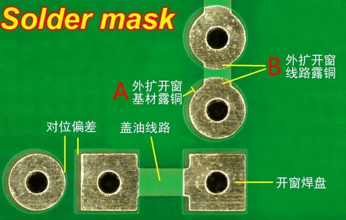
In the design and manufacturing of modern electronic products, the Printed Circuit Board (PCB) plays a crucial role. Among the many process and design parameters of a PCB, "soldermask expansion" may seem like a minor parameter, but it directly affects soldering quality, manufacturing yield, and the long-term reliability of the circuit board.
What is Solder Mask?
The PCB solder mask, also called the window layer or green solder mask layer, is the area on the PCB where green solder mask is applied. This solder mask layer uses negative film output, so when its shape is mapped onto the board, it doesn't appear as green solder mask; instead, the copper is exposed. The solder mask layer is important in controlling soldering defects during reflow soldering. The main uses of the solder mask layer include:
Preventing solder bridging: During the soldering process, automatic soldering may create solder bridges between adjacent pads. The presence of the solder mask layer effectively avoids this short-circuit risk.
Protecting the copper surface: Preventing oxidation of exposed copper foil and improving environmental resistance.
Enhanced Insulation: In high-density circuits, the solder mask provides additional insulation protection.
Defining Pad Areas: In surface mount technology (SMT), the openings in the solder mask define the area that can be covered by solder.
The solder mask typically covers the entire PCB surface, except for areas like pads and vias that need to contact the outside, where openings expose the copper surface.

soldermask
Definition of soldermask expansion:
Solder mask expansion refers to the opening size of the solder mask on a printed circuit board (PCB) being slightly larger than the pad. This ensures that the solder can correctly fill the pad during soldering, preventing solder joint misalignment or cold solder joints. This expansion is usually set during the design phase to ensure soldering reliability. This specification is commonly referred to as soldermask expansion and can be positive, negative, or zero.
Positive Solder Mask Expansion: When there is a gap between the end of the solder mask and the outer circumference of the uncovered pad, it is called positive solder mask expansion.
Zero Solder Mask Extension: This value is zero when there is no gap or spacing between the solder mask and the pad.
Negative Solder Mask Extension: This value is negative when the solder mask overlaps with the pad area.
Why is Solder Mask Extension Necessary?
PCB component pads need exposed copper, so a window needs to be created in the solder mask. This means the area where copper needs to be exposed will not be covered by the solder mask. Furthermore, we need to prevent the solder mask from covering the exposed copper area of the pad, which would worsen the pad's solderability.
If the area of the solder mask window is the same size as the pad, due to PCB manufacturing tolerances, it's unavoidable that the solder mask will cover the pad. Therefore, to accommodate the PCB manufacturer's process deviations, we generally make the solder mask window area larger than the actual pad by a certain size. Current PCB manufacturers recommend (4mil or 0.1mm).
So, should we set the solder mask tolerance precisely when creating the PCB footprint library? Actually, it's sufficient to keep the solder mask size consistent with the PCB pad size during footprint creation. Some PCB EDA software allows options to automatically expand the solder mask when exporting Gerber data, or CAM software can easily handle soldermask expansion.
Therefore, when creating the PCB footprint library, simply ensure the solder mask matches the actual pad size.

soldermask expansion
What risks does excessive soldermask expansion pose? Excessive expansion is also undesirable and may lead to:
1. Disappearance of solder mask bridges (Soldermask Dam disappearance)
For example, in a 0.5 mm pitch BGA, the solder mask bridge between two pads may disappear due to excessive expansion, causing solder bridging and short circuits.
2. Excessively large solderable area and excessive solder
This results in abnormally large solder joints, failing to meet IPC soldering standards.
3. Impact on Soldering Positioning of Precision Components
Especially for QFN/PQFN packages, insufficient solder mask can cause solder overflow.
Therefore, solder mask extension must strike a balance between precision and safety.
While soldermask expansion is only a fundamental parameter in PCB design, it is closely related to manufacturing processes, soldering quality, and product reliability. Properly setting solder mask extension can not only improve soldering yield but also significantly enhance the reliability and stability of the PCB. Professional PCB design must consider multiple factors such as component type, manufacturing tolerances, solder mask bridge width, and application scenario to achieve high-quality engineering results.
As modern electronic products evolve towards higher density, thinner profiles, and higher speeds, soldermask expansion design will become increasingly sophisticated. Understanding its principles and design methods is crucial for improving PCB design capabilities.