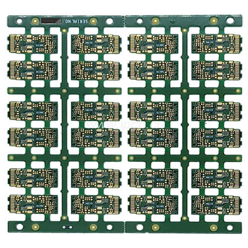
What is HDI? HDI PCB stands for High Density Interconnect PCB, also known as High Density Interconnect Board, which is a high-density circuit board with high line distribution density. Adopting micro blind hole technology. HDI PCB has internal and external circuits, and each layer of circuit is connected internally through processes such as drilling and metallization inside the holes.
HDI PCBs are generally made by stacking, and the more times they are stacked, the higher the technical level of the board. Ordinary HDI PCBs are basically first-order, while high-precision HDI PCBs use two or more blind hole stacking processes to become second-order PCBs. For every additional blind hole stack in HDI PCB, the order increases by one order. Each layer with blind hole stacking is an Anylayer HDI PCB. HDI PCB adopts advanced PCB technology, such as stacking holes, electroplating filling holes, laser drilling and other manufacturing processes.
When the PCB density increases by more than 8 layers, the cost of HDI will be lower than traditional complex compaction processes. HDI PCB is beneficial for the application of advanced construction technology, with higher electrical performance and signal accuracy than traditional PCB. Additionally, HDI boards have better improvements in RF interference, electromagnetic wave interference, electrostatic discharge, thermal conductivity, and other aspects.

HDI PCB Products
Electronic products are constantly developing towards high density and high precision. The so-called 'high' not only improves the performance of the machine, but also reduces its size. High density integration (HDI PCB) technology can make the final product design smaller, meeting higher electronic performance and efficiency standards. Currently, many popular electronic products, such as mobile phones, digital cameras, laptops, and automotive electronics, use HDI PCB boards. With the upgrading and replacement of electronic products and market demand, the development of HDI PCB boards will be very rapid.
PCB Introduction
PCB (Printed Circuit Board) is an important electronic component that serves as the support for electronic components and the carrier for electrical connections.
The main function of this device is to avoid manual wiring errors due to the consistency of the same printed circuit board when electronic devices adopt it. The automatic insertion or installation of electronic components, automatic soldering and automatic detection of electronic components have been achieved, ensuring the quality of electronic equipment, improving labor productivity, reducing costs, and facilitating maintenance.
Is a PCB with blind holes called HDI PCB?
HDI PCB is a high-density interconnect circuit board. The blind hole electroplating secondary pressure plate is an HDI PCB, which can be divided into first, second, third, fourth, and fifth order HDI PCB circuit boards. For example, the iPhone 6 motherboard is a fifth order HDI PCB circuit board.
Simple burial pits may not necessarily be HDI PCBs.
How to distinguish the first, second, and third order of HDI PCB.
The first order is relatively simple, and the process is easy to control.
The second step starts to have problems, one is alignment, and the other is drilling and copper plating. There are many second-order designs, one of which is that each order is wrong. When connecting the second adjacent layer, it is necessary to connect the wires of the middle layer, which is equivalent to two primary HDI circuit boards.
The second is that two first-order holes overlap, and the second-order holes coincide. Processing is similar to first-order, but there are many key points that require special control, namely the above points.
Thirdly, rush directly from the outer layer to the third layer (or n-2 layer). This process is very different from the front, as drilling is more difficult.
For the third order, the second simulation is.
The difference between HDI PCB and PCB Board
Common PCB boards are mainly made of epoxy resin and electronic grade glass cloth FR-4. Generally speaking, HDI PCB should use adhesive backed copper foil. Because laser drilling cannot open glass cloth, non glass fiber backed copper foil is generally used, but now high-energy laser drilling machines can break through 1180 glass cloth. In this way, it is no different from ordinary materials.