What PCB files do I need to provide to the PCB fabrication to produce a PCB? To produce a PCB, you need to provide PCB manufacturers with the following information:
1.Gerber files (Gerber flies) are used for the production files of the PCB factory, and are usually compressed and packaged independently.
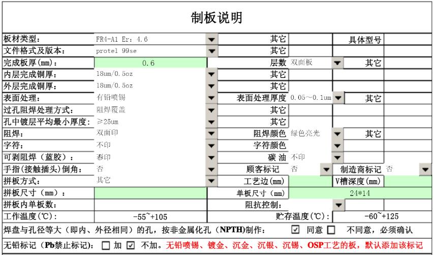
2.PCB process description file used to illustrate the PCB board process technology, such as board type, thickness, plating process, standards, etc., generally PDF format.
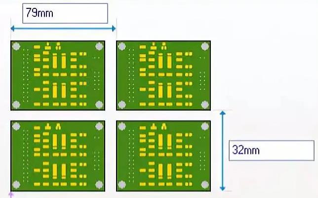
3.PCB board diagram is a single board into a number of pieces together with the production, to save production time, improve production efficiency, reduce the waste of boards, reduce costs.
Gerber flies, Gerber file description
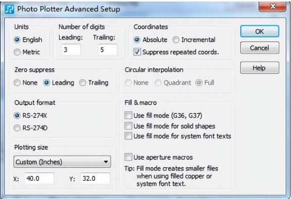
PCB layout board to check for errors in the case of Gerber files, drawing type.Drilling.Silk-screen printing or wiring and the related output device settings are called CAM files.
Default settings do not need to change, especially the output format is RS-274-X, you can use the modeless command @CAMDOCS shortcut output gerber file, pay attention to the solder mask layer, the default zoom 10, remember to delete.Check the naming and layer sections of other layers one by one.
1.Routing layer (Routing/Split Plane): board alignment (Trace).Solder pads (Pad).Copper (Copper) and through-hole (Via), etc., the board has several layers, there are several corresponding files.
2.Green oil window layer (Solder mask): that is, the board needs to be exposed to the area of copper, this has two layers (Top and Bottom).
3.Silkscreen layer (Silkscreen): that is, the board needs to identify the information, such as component number (Reference Designator).Polarity mark, version information.Company logo, etc.This also has two layers (Top and Bottom).
4.Drill Layer (NC drill and Drill drawing): There are several Via types in board design, corresponding to several NC drill files, but only one Drill drawing file.

Gerber flies out
PCB process description file
1.PCB material: the first to explain the PCB production material is what is needed, the most common is to use FR4, the main material is epoxy resin stripped fibre cloth board, Audemars Piguet Circuits also have the use of ceramic substrate, metal substrate and other PCB materials.
2.Board layer: to explain the number of layers you make PCB board.The pcb board is made of different layers, the price will make a difference, and PCB sampling process is similar.
3.Soldermask colour: there are many kinds of colours, you can also choose according to the company's requirements, the general is green.
4.Silk-screen colour: PCB silk-screen font and border colour, generally choose white.
5.Copper thickness: generally according to the current of the PCB circuit to carry out scientific calculations of copper thickness, generally the thicker the better, but the cost will be higher, so the need for a reasonable balance.
6.Whether the vias are covered with soldermask: Soldermask is to insulate the vias, otherwise it is to leave the vias uninsulated.
7.Surface treatment technology: spray tin.Gold plating.Gold plating, OSP, silver and so on.
8.Whether there are impedance requirements, pointing out the PCB impedance line.Requirements of the PCB stacking layer, etc.Audemars Piguet can calculate the impedance value for the customer and give a reasonable stacking layer.
9.Quantity: Specify the number of PCBs to be produced.
10.Whether there are other special requirements are also pointed out.

PCB process description file
Printed Circuit Board (PCB)
PCB refers to allow PCB manufacturers to directly connect a small PCB board into a whole piece.
Why do we need to connect the boards? What are the advantages of the PCB?
1.To meet the production demand. Some PCBs are too small to meet the fixture requirements, so they need to be put together for production.
2.Improve the efficiency of SMT soldering. Only one SMT can complete the soldering of multiple PCBs.
3.Improve cost utilisation. Some PCB boards are shaped, the patchwork can be more efficient use of PCB board area, reduce waste and improve the cost of utilisation.

Printed Circuit Board (PCB)
Abbey Circuit can connect the boards according to the production situation of the factory, the principle of saving data,improve the efficiency and reduce the cost of PCB.
Above is the production of PCB for everyone to share the need to provide what PCB files to the PCB manufacturer,the production of a piece of PCB,need to provide information to the PCB factory including Gerber files (Gerber flies), PCB process description file,PCB connecting the board diagrams.