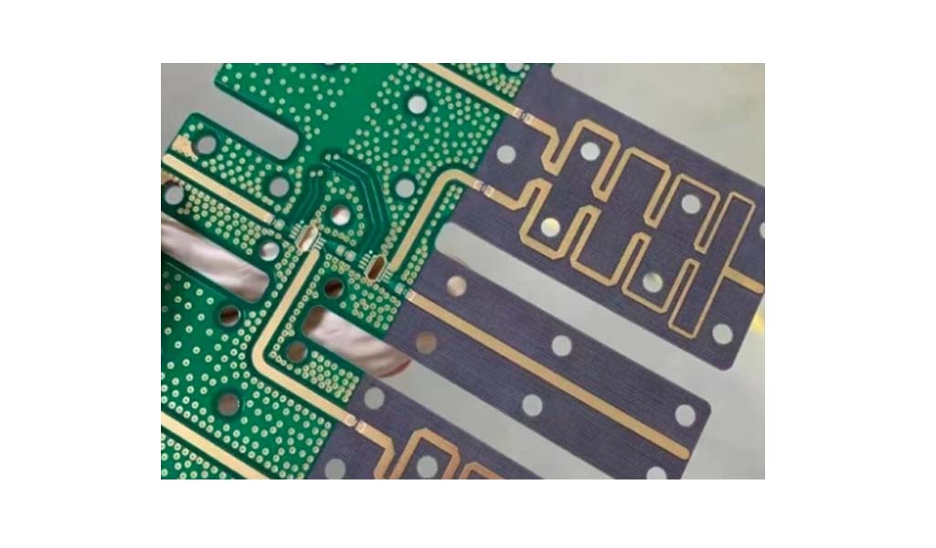
Designing high frequency PCBs can be challenging; as a PCB designer, you need to understand the physics and implications of high frequency PCB design. Various elements are required to create such designs. These elements include routing, component placement, and grounding. Proper spacing between traces is also an important aspect of PCB design. Although there is much debate about routing angles, most designers agree on a 45-degree angle. This angle reduces capacitance. Optimal high frequency PCB design includes correct spacing and component placement.
When designing a high frequency PCB, it is important to choose the right material that can meet the high frequency design requirements. For cost reasons, a hybrid design should be considered, where more expensive, faster materials are used only on the layers where they are needed; the rest of the board is made of FR-4.
Select components rated for high frequencies:
Check datasheets to confirm HF suitability
Watch out for marginal components that are not fully characterized
Select component packages with low inductance and parasitics:
Avoid long leads
Favor small SMT packages
Watch out for parasitic capacitance
Position noise-sensitive components wisely:
Keep away from high-speed lines and interfaces
Provide shielding if needed
Position components for shorting lines:
Place components with high-speed interactions nearby
Minimize overall trace lengths
Putting the right components in the right place from the start allows for optimal routing.
Use isolated routing for high frequency PCB design:
Another consideration is how to route between components. However, you may also need strategies to isolate traces between different board sections and around individual interconnects to prevent interference. Some strategies include:
Coplanar waveguide routing on surface layers, especially for tracks between components, to feed lines, or to coaxial connectors.
If you have enough layers, consider leaving one layer for stripline routing. Proceed with caution, as vias can cause problems at very high frequencies.
Placing a ground fence around the RF power plane can provide a good level of suppression, as it creates two out-of-phase radiators.
Consider using bandgap structures to provide isolation, as these can be printed directly onto high-frequency PCBs.

Stackup is an important factor in high-frequency circuit design. The number of layers and their arrangement will directly affect the performance of the signal. A standard high-frequency PCB stackup will include a power layer, multiple ground layers, and a signal layer between these power and ground layers. To avoid crosstalk in such a stackup, always use a ground layer to isolate the signal layer. Likewise, increase the distance between signal layers to minimize crosstalk. Other high frequency PCB design rules for stackup include the use or vertical orientation of adjacent layers, and the use of microvias to reduce inductance and improve signal integrity. Digital signals should also be separated from analog signals for better performance.
When designing a high-frequency board, it is critical to keep impedance under control. To ensure this, several design rules must be followed. First, make sure you use the correct trace width for the desired impedance. Shorter traces help reduce inductance, while wider traces help increase impedance. Use the 3 or 2W rule to separate traces and control their impedance. This rule states that for optimal impedance control, the spacing between traces should be at least 3 or 10 times their width. As mentioned earlier, using a ground plane can reduce crosstalk and signal loss. Placing the ground trace directly underneath the signal trace will help achieve better impedance control. Pay attention to layer transitions when routing high-frequency circuit signals. Ensure the transition from one layer to another is as smooth as possible, using microvias to avoid signal reflections.
Applications of high-frequency PCB design involve industries that rely on fast, accurate signal transmission and processing. As technology continues to advance, the demand for high-frequency electronics will only grow, further highlighting the importance of mastering this design principle. High frequency PCB design is essential to ensure the optimal performance of modern electronics. As the demand for faster and more efficient electronic devices continues to grow, the need for reliable high-frequency PCBs becomes critical.