A Trustworthy PCB and Electronic Manufacturing Enterprise! Contact Us



For high-speed and mixed-signal hardware designers, mastering a reliable 6 layer pcb stackupis fundamental to stabilizing signal integrity, power distribution performance, and EMC compliance. Many layout engineers rely on layer count upgrades to solve routing congestion, yet overlook that stackup architecture dominates circuit performance far more than trace routing itself. Four-layer PCBs hit obvious bottlenecks in high-density, high-speed, and multi-voltage designs, while eight-layer and higher multilayer boards introduce unnecessary layer redundancy and elevated engineering costs. A well-tuned 6 layer pcb stackup delivers the ideal balance of routing flexibility, planar integrity, and cost control, making it the most versatile mid-tier structure for modern embedded and industrial circuit design. This article breaks down practical stackup logic, layer allocation strategies, high-speed design rules, and common technical pitfalls for peer hardware engineers.
To understand the value of six-layer structures, it is necessary to clarify the applicable boundaries of conventional PCB layer configurations. Single and double-layer boards are reserved for simple low-voltage DC circuits and basic switching hardware, where signal speed, crosstalk, and electromagnetic radiation pose no design risks. Standard four-layer PCBs adopt the classic SIG/PWR/GND/SIG stacking mode, which works well for general MCU control circuits, low-speed serial communication systems, and basic power supply modules. This structure provides basic plane separation for power and ground, meeting ordinary EMC and power decoupling requirements.
However, four-layer architecture faces inherent limitations in complex design scenarios. When designs involve high-I/O controllers, FPGAs, DDR storage circuits, analog signal sampling, and multi-domain power supply systems, surface routing resources become extremely saturated. Top and bottom layers bear all component placement, high-speed signal wiring, and partial power trace layout, forcing high-speed differential lines, clock signals, and low-speed control traces to run in parallel. This crowded layout triggers severe crosstalk, discontinuous signal return paths, and insufficient high-frequency power decoupling. Additionally, four-layer boards struggle with effective isolation between analog and digital grounds, frequently introducing switching noise into precision sampling circuits and degrading overall system stability.
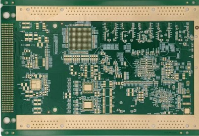
It is in these high-demand scenarios that a standardized 6 layer pcb stackup fundamentally resolves the pain points of four-layer design without the cost overhead of higher-layer boards. A common misconception among junior engineers is that six-layer PCBs merely add two extra signal routing layers. In practice, the core optimization of the 6 layer pcb stackup lies in reconstructing power and ground plane pairing, building complete reference planes for high-speed signals, and separating multi-voltage power domains and mixed-signal routing spaces. This structural optimization comprehensively improves signal integrity (SI), power integrity (PI), and electromagnetic compatibility, rather than simply expanding routing channels.
Before implementing formal stackup design, engineers must recognize and avoid the worst-case six-layer configuration: SIG/PWR/SIG/SIG/GND/SIG. This unoptimized stackup is structurally defective for almost all high-speed and mixed-signal applications. Adjacent inner signal layers create severe mutual crosstalk with no shielding ground plane between them. Meanwhile, the independent power layer lacks a tightly coupled ground reference plane, resulting in extremely poor PDN high-frequency decoupling capability and unstable power supply transient response. This structure is only viable for pure DC static circuits with no high-speed switching characteristics and should never be adopted for industrial, communication, or precision analog designs.
In conventional engineering practice, the most universal and performance-balanced6 layer pcb stackup follows the symmetrical sequence: Top(SIG) – GND – PWR – SIG – GND – Bottom(SIG). This stackup is widely recognized as the standard configuration for mid-complexity hardware designs, applicable to high-speed embedded systems, FPGA core circuits, mixed-signal acquisition boards, and multi-voltage power supply systems. Its symmetrical structure ensures planar stability, uniform dielectric loss, and consistent impedance characteristics, laying a solid foundation for standardized high-speed design.
The primary advantage of this stackup is the proximity of outer signal layers to complete ground planes. All critical high-speed signals, including differential transmission lines, clock signals, and high-speed interface traces, can be arranged on the top and bottom layers. The adjacent integrated ground plane provides the shortest low-impedance return path, effectively controlling signal impedance continuity, suppressing line crosstalk, and reducing electromagnetic radiation. The inner power layer independently undertakes all multi-voltage power distribution work, separating power planning and signal routing physically to avoid resource conflicts.
This inner power plane solves the core difficulty of multi-voltage fanout for high-density BGA and FPGA devices. Advanced controllers and programmable gate arrays usually contain multiple independent voltage domains, with a large number of pins dedicated to power and ground connections. In four-layer designs, power traces must be routed on limited surface layers, causing crowded fanout, overlapping power tracks, and unpredictable EMI coupling risks. In the optimized six-layer stackup, all power pins connect vertically to the inner power layer via vias, while ground pins link to the adjacent complete ground plane. This vertical fanout mode simplifies layout greatly and eliminates the interference risks caused by planar interleaving of different power rails.
Designers can partition the inner power plane according to voltage domain requirements to form independent power areas for core voltage, IO voltage, analog voltage, and reference voltage. Each power domain is relatively independent without cross-overlapping, which fundamentally reduces low-frequency coupling and high-frequency noise interference between different power supplies. Moreover, the tightly coupled power-ground plane pair forms a natural plate capacitor, providing excellent high-frequency decoupling characteristics. This structure effectively suppresses power ripple and instantaneous voltage drop during high-speed chip switching, optimizing the overall power distribution network performance.
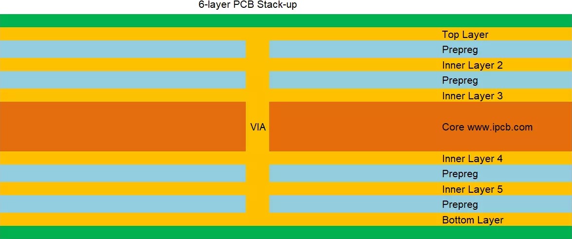
It is important to clarify that the inner power layer does not completely replace surface power wiring. In actual layout work, local high-current power circuits can still be laid out through thick copper traces or copper pouring on surface signal layers. The inner plane undertakes mainstream multi-voltage power distribution, while surface wiring supplements partial high-current scenarios, forming a flexible and complementary power layout system.
Six-layer structures also show unique advantages in mixed-signal design. Unlike four-layer boards that struggle with thorough digital-analog isolation, six-layer stackups support layered partitioning of analog and digital circuits. The surface layer can be independently used for analog interface and precision sampling signal routing, matched with a complete ground shielding layer. The inner signal layer is dedicated to low-speed digital control wiring, realizing physical separation of analog weak signals and digital switching signals. Analog ground and digital ground adopt reasonable partition and single-point grounding design to eliminate ground loop noise, greatly improving the acquisition accuracy and stability of analog circuits.
In daily design work, engineers need to avoid a typical invalid optimization, namely the pseudo six-layer structure. This error refers to simply superposing two signal layers on the basis of four-layer boards without optimizing power and ground plane pairing. Although the layer count increases, there is no complete coupled power-ground plane, so SI, PI, and EMC performance cannot be effectively improved. This blind layer upgrade only increases production costs without bringing performance gains, which is a typical unreasonable design and needs to be strictly avoided in formal project development.
In terms of routing specifications, all EMC and integrity design principles applicable to mainstream multilayer boards can be migrated to six-layer designs, with targeted optimization based on stackup characteristics.
For formal project iteration and mass production, stackup design must fully cooperate with DFM manufacturability verification. Before finalizing the 6 layer pcb stackup, designers need to confirm key parameters including board thickness, dielectric medium characteristics, copper thickness, and impedance tolerance according to conventional manufacturing processes. Different process parameters will affect the impedance matching of 50Ω single-ended signals and 100Ω differential signals. Only by docking stackup parameters with processing standards in advance can impedance mismatch and batch performance inconsistency be avoided in mass production.
Simulation verification is an indispensable link to ensure design reliability. After completing stackup planning and preliminary layout, engineers can adopt professional simulation tools to carry out comprehensive SI, PI, and EMC analysis. Signal integrity simulation verifies signal reflection, transmission delay, line crosstalk, and impedance matching status. Power integrity simulation detects PDN impedance distribution, instantaneous voltage drop, and resonant defects of power planes. EMC simulation predicts conducted and radiated interference risks in advance, realizing pre-adjustment in the design stage and avoiding repeated board modifications caused by late-stage test failures.
Overall, the six-layer PCB has become the optimal mid-tier solution for complex hardware design due to its moderate cost, flexible layout space, and excellent comprehensive performance. The core of high-quality six-layer design is never the simple superposition of layers, but the scientific and reasonable construction of stackup architecture. Through standardized plane pairing, reasonable voltage domain partitioning, strict high-speed wiring constraints, and systematic simulation verification, engineers can effectively improve the stability, anti-interference ability, and yield of hardware circuits.
For most embedded control, industrial signal acquisition, and high-speed transmission circuit designs, upgrading from four-layer to standardized six-layer stackup is the most cost-effective performance optimization scheme. Abandoning defective stackup structures and pseudo-multilayer designs, and adhering to stackup-first design thinking can effectively reduce later-stage EMC rectification costs and project iteration cycles, providing reliable technical support for standardized and high-quality hardware design.