A Trustworthy PCB and Electronic Manufacturing Enterprise! Contact Us



In modern industrial automation, the demand for precision, speed, and reliability has never been higher. Whether it is automated optical inspection (AOI) on high-speed SMT lines, robotic guidance in automotive manufacturing, or dimensional metrology in semiconductor fabrication, machine vision acts as the eyes of the smart factory. At the heart of these sophisticated vision systems lies a critical component: the Camera PCB Module.
For hardware engineers, optical designers, and system integrators, selecting or custom-designing the right Camera PCB Module can make or break an entire machine vision project. Moving beyond off-the-shelf box cameras often requires embedded board-level solutions to meet strict spatial, thermal, and performance constraints. This article dives deep into the engineering considerations, architectural trade-offs, and integration strategies for deploying a Camera PCB Module into demanding industrial machine vision environments.
1. Why Board-Level Vision Matters in Industrial Automation
Traditional enclosed industrial cameras are robust, but their bulky housings, fixed connector orientations, and rigid thermal paths frequently clash with the miniaturization trends of modern automated equipment. Multi-axis robots, handheld inspection probes, and compact embedded processing units leave very little room for standard hardware.
A board-level Camera PCB Module separates the raw imaging stack from unnecessary external housing, offering unmatched mechanical flexibility.Space Constraints: Engineers can mount the sensor board directly onto optical chassis or inside tight robotic end-effectors.Custom Optical Integration: Eliminates redundant glass filters or mounts, allowing direct integration with specialized lenses (such as M12, C-mount, or custom liquid lenses).Optimized Bill of Materials (BOM): Reduces redundant enclosures and external interface conversion chips, lowering the overall cost for scaled OEM production.
2. Core Technical Specifications for Industrial Vision
When evaluating or designing a Camera PCB Module for industrial applications, engineering teams must balance several interdependent parameters. Compromising on one often impacts the entire imaging pipeline.
Sensor Selection: Global vs. Rolling Shutter Industrial machine vision almost exclusively relies on CMOS image sensors. The choice between shutter types is dictated by motion:Global Shutter: Essential for high-speed applications (e.g., conveyor belts, high-speed sorting). All pixels expose simultaneously, preventing motion artifacts and image skew. Rolling Shutter: Suitable for stationary or slow-moving inspection targets where cost optimization and higher pixel density are prioritized.High-Speed Data InterfacesMoving uncompressed high-resolution video streams from the Camera PCB Module to the host processor or FPGA requires robust data interfaces. Common choices include:MIPI CSI-2: Highly popular in embedded vision systems due to its low latency and high bandwidth, directly interfacing with modern edge processors (like NVIDIA Jetson or NXP i.MX series).USB 3.0 / USB3 Vision: Plug-and-play capability with standardized protocols, ideal for PC-based machine vision systems. GigE / 10GigE (via interface bridge): Best for long-distance cable runs in large factory environments.
3. Key Applications in Industrial Machine Vision
Where do engineers deploy these specialized board-level cameras? Their versatility shines across several core verticals of industrial automation:
Automated Optical Inspection (AOI) & SMTIn electronics manufacturing, printed circuit boards (PCBs) must be inspected for solder defects, missing components, and tombstoning at lightning speeds. A high-resolution Camera PCB Module integrated into an AOI gantry captures micro-details under specialized lighting (e.g., coaxial, ring, or dome lighting) to feed real-time defect-detection algorithms.Robotic Pick-and-Place & Guidance Industrial robots require real-time spatial awareness to locate, align, and pick up irregularly placed components. Board-level cameras mounted directly near the robotic gripper provide eye-in-hand capabilities, executing high-accuracy coordinate transformations without adding excessive payload weight to the robotic arm.Surface Defect Metrology and Semiconductor PackagingFrom wafer inspection to metal surface flaw detection, machine vision systems demand high dynamic range (HDR) and low-noise performance. Custom Camera PCB Modules allow engineers to couple specialized sensors (such as UV or NIR-sensitive sensors) to detect sub-surface or microscopic material fractures that standard visible-light cameras miss.
4. Engineering Challenges and Mitigation Strategies
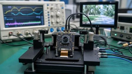
Integrating a bare-board imaging module into a harsh industrial setting introduces unique hurdles that go beyond standard software development.Thermal ManagementIndustrial environments can experience wide temperature fluctuations, and image sensors are notoriously sensitive to thermal noise (dark current).Design Tip: Ensure adequate copper planes on the Camera PCB Module layout to dissipate heat away from the sensor die. For enclosed multi-board sandwiches, incorporate thermal pads that interface with the outer metallic machine chassis.Signal Integrity (SI) and Electromagnetic Interference (EMI)High-speed differential lines like MIPI or USB pass massive amounts of high-frequency data. In factories filled with high-voltage servo motors and switching power supplies, EMI can easily corrupt image frames.Design Tip: Implement strict length-matching for differential pairs, use continuous ground planes beneath high-speed traces, and place adequate decoupling capacitors close to the sensor power pins (VDD, VAA, etc.).Optics and Mechanical AlignmentUnlike enclosed cameras with factory-calibrated lens mounts, a modular design requires precise mechanical tolerancing. A tilt of even a fraction of a millimeter in the lens holder relative to the sensor plane will cause uneven focus across the field of view (FOV). Precision active alignment during manufacturing is vital for high-end metrology applications.
5. Conclusion
The success of a machine vision system frequently relies on the reliability of its foundational components. By utilizing a well-engineered Camera PCB Module, hardware developers can bypass the limitations of bulky commercial cameras, achieving tight mechanical integration, low latency, and superior image acquisition tailored precisely to their industrial application.As smart factories continue to push for higher speeds and deeper AI integration at the edge, mastering board-level camera design and system integration will remain a core competency for advanced automation engineers.