A Trustworthy PCB and Electronic Manufacturing Enterprise! Contact Us



A Power Supply PCB Board is the "energy heart" of any electronic device — the circuit responsible for power conversion and regulated voltage delivery. Its quality has a direct bearing on whole-system stability, which makes power supply PCB design a critical control point for both product performance and appliance-industry supply chain cost.
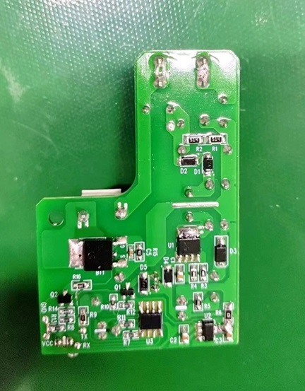
Where Power Supply PCB Boards Show Up
As the dedicated carrier for power conversion and distribution, the Power Supply PCB Board shows up in nearly every category of electronics. On the consumer side, that means TVs, refrigerators, air conditioners, phone fast-chargers, and laptop adapters. On the industrial side, it covers frequency converters, industrial control mainboards, and instrumentation power supplies. It also extends into telecom base stations, server power supplies, solar inverters, EV on-board chargers (OBC), medical monitors, and aerospace-grade power units. Requirements vary by application — power density, voltage rating, thermal efficiency, and EMC performance are all weighted differently — but the core mission is constant: deliver clean, stable, safe power to everything downstream.
Getting the power supply PCB layout right up front is what keeps a product from running into excessive temperature rise, uncontrolled interference, safety-compliance failures, or mass rework down the line. Power board design is never just component placement and routing — it's about finding the optimal solution across four coupled domains at once: power flow, signal flow, heat flow, and electromagnetic field. High-voltage, high-current loops coexisting with weak sampling signals on the same board is exactly what makes power PCB layout fundamentally different from a standard digital board — and why even small oversights can keep a finished product from meeting spec.
Five Core Design Priorities
1. Zone-based layout first. Follow the power flow strictly in a straight line: high-voltage input → EMI filtering → rectifier bridge → power conversion → secondary-side rectification → output filtering. Keep primary and secondary circuits physically isolated with adequate safety clearance, and place core components — transformer, power devices, electrolytic capacitors — close together to minimize roundabout routing.
2. Trace current-carrying capacity and loop control. High-current main loops should follow the "short, straight, wide" principle, sizing trace width against the baseline standard of roughly 1A per 10mil (0.25mm). Keep the positive and negative traces of each power loop running parallel and close together to minimize loop area — the most effective way to cut radiated emissions and trace losses at the source.
3. Grounding architecture. Route power ground and signal ground separately, converging them at a single point — typically at the main filter capacitor's pin — to prevent voltage drop from high current on the ground trace from corrupting sampling accuracy. Broad ground pours serve double duty here, providing both shielding and heat dissipation.
4. Safety and insulation design. Creepage distance and clearance between primary and secondary circuits must meet UL, IEC, or GB safety standards as applicable. Slotting in high-voltage regions, and the placement of safety capacitors and Y-capacitors, both require careful calculation rather than rule-of-thumb placement.
5. Thermal management. Spread heat-generating components — transformer, MOSFETs, rectifier diodes — across the board rather than clustering them, extend copper pours evenly beneath them, and reserve heatsink mounting locations where needed to avoid localized heat buildup that accelerates capacitor aging.
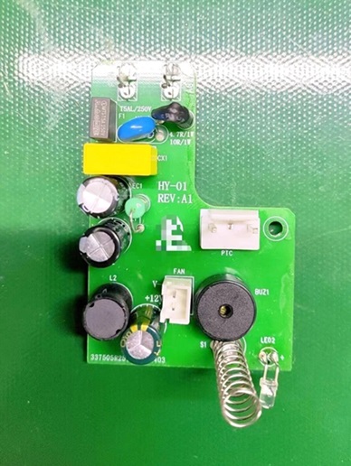
Why Home Appliances Standardize on Single-Layer Boards
Once you understand the design logic above, an interesting pattern emerges across the industry: crack open the power supply inside a TV, air conditioner, or washing machine — whether it's a Sony, a Samsung, or a leading domestic appliance brand — and you'll almost always find a single-layer power supply PCB, not the higher-spec double-sided or multilayer alternative. That's not a corner being cut; it's a choice validated by decades of industry practice, and it rests on four underlying reasons.
Topology maturity matches single-layer complexity. Home appliance power supplies overwhelmingly use standardized, well-understood topologies like flyback and forward converters — few components, fixed part selection, and clean routing logic. A layout with components and routing on opposite sides, with the rare crossover handled by a single jumper resistor, is fully achievable on a single-sided board. There's no need to pay for extra vias or lamination when single-layer capability already covers 100% of the requirement.
No-via construction actually improves long-term reliability. A power supply PCB board operates continuously under high voltage, high current, and sustained temperature rise — conditions where vias are the weakest point in the entire structure. Repeated thermal cycling combined with electrochemical corrosion can crack the via barrel's copper plating, driving contact resistance up or causing outright open/short failures. A single-layer board eliminates via failure risk entirely by design, with every solder joint on the same side — a meaningful advantage for long-term stability and service life.
Production and rework efficiency are both better. Single-layer boards skip drilling, copper deposition, and plating steps entirely, which means a shorter production flow, higher yield, and simpler failure tracing. On the service side, even a full factory-return repair benefits: with every trace and solder joint visible from a single side, there's no need to cross-reference layer files or flip the board repeatedly — continuity testing and touch-up soldering are both dramatically faster than on a double-sided board.
It's the cost-performance sweet spot under specialized manufacturing. Most appliance OEMs don't build their own power boards in-house — they specify requirements and source from dedicated power supply manufacturers at scale. These specialized manufacturers have spent decades refining their designs and processes, pushing single-layer power supply cost down to its practical floor while holding reliability and consistency at a high, repeatable level. Given that appliance products only need to be "stable enough, with adequate service life," the single-layer board is the natural, industry-wide answer.
There's no rule in electronics that says "more advanced is automatically better." Selecting and designing a Power Supply PCB Board is fundamentally about finding the right balance between functional requirements, long-term reliability, and overall cost — and that balance, more than any spec sheet, is what good industrial design has always been about.