A Trustworthy PCB and Electronic Manufacturing Enterprise! Contact Us



When it comes to advanced high-speed digital design, optimizing your pcb board stackup is the absolute foundation for ensuring flawless signal integrity and mitigating electromagnetic interference before a single trace is routed.
At its fundamental level, a stackup refers to the precise physical arrangement of conductive copper layers and insulating dielectric prepreg or core materials from top to bottom. This is a definitive, once-and-done structural decision locked in the moment lamination finishes. If you are scaling up production for modern electronics, partnering with an expert provider for multi-layer pcb manufacturing solutions ensures that your layer configurations are properly engineered right from the start to prevent critical manufacturing defects such as severe board warpage and thermal stress failures.
Mastering high-speed layouts requires adhering to strict physical and electrical rules. Every high-speed signal layer must sit adjacent to an uninterrupted, continuous reference plane to provide a low-impedance return path, stabilize characteristic impedance, and minimize crosstalk. Furthermore, maintaining strict layer symmetry across a central axis prevents thermal distortion during reflow soldering. To bring these complex architectural layouts to life with precise copper weight distribution and strict impedance tolerances, engineers often rely on advanced custom pcb fabrication services equipped with state-of-the-art lamination presses.
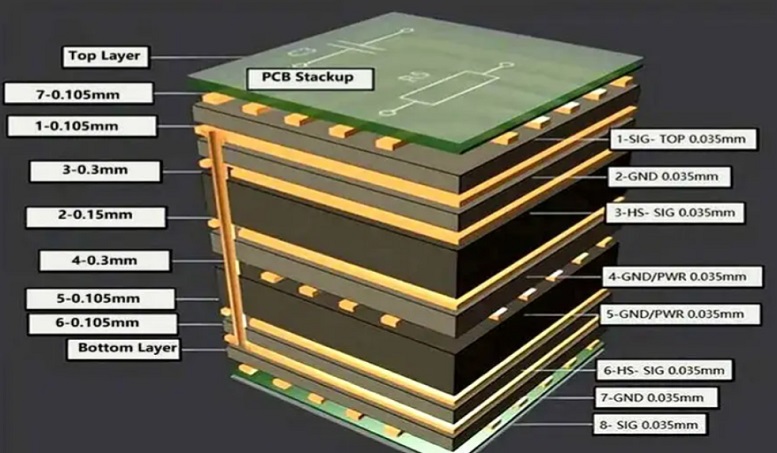
Why is this structural planning so critical? In modern hardware engineering, a poorly planned pcb board stackup can completely cripple system performance. It directly governs the four pillars of circuit board success: Signal Integrity (SI), Power Integrity (PI), Electromagnetic Compatibility (EMC), and Design for Manufacturability (DFM). Once a board is laminated, no amount of post-routing optimization or firmware tuning can fully salvage a design suffering from broken return paths or uncontrolled reference switching.
Let's dive deeper into the core principles of layer arrangement. The first golden rule dictates that signal layers must always be close to their reference planes. When a high-speed signal transitions from a driver to a receiver, the return current mirrors its path right beneath the trace on the nearest ground or power plane. If a split or gap interrupts this plane, the return current is forced to take a detour, expanding the current loop area and causing catastrophic electromagnetic radiation spikes. Additionally, power and ground planes should be paired tightly together to form a parallel-plate capacitance structure, offering low-inductance decoupling that subdues high-frequency voltage ripples.
Different applications demand different layer counts. A standard 4-layer board is typically reserved for low-to-medium speed embedded systems, whereas a well-designed pcb board stackup for 6 or 8 layers serves as the gold standard for high-performance computing, PCIe interfaces, and DDR memory routing. In these multi-layer architectures, inner signals are safely tucked away as striplines between two reference planes, providing double-sided electromagnetic shielding. For ultra-high-speed data centers, AI accelerators, and 112G PAM4 routing running on 10 to 40+ layers, alternating signal-ground-power configurations become mandatory to maintain signal fidelity across dense networks.
Choosing the right materials is just as important as the layer sequence itself. High-speed design demands careful consideration of dielectric constants (Dk) and dissipation factors (Df). While standard FR-4 materials are acceptable for low-frequency applications, high-frequency systems require low-loss or ultra-low-loss laminates (such as Megtron or Rogers series) to minimize insertion loss over long traces. Furthermore, high-frequency design must account for copper foil roughness. Standard rolled copper introduces high skin-effect losses at gigahertz frequencies, making low-profile (VLP) or ultra-low-profile (HVLP) copper foils essential for modern high-speed transmission lines.
Electromagnetic interference (EMI) management relies heavily on structural design choices. By nesting power planes between solid ground planes and implementing stitching via walls along high-speed differential pairs, engineers can effectively trap electromagnetic fields within the board stack. On the manufacturing side, maintaining balanced copper densities across layers prevents uneven resin flow during pressing. Symmetrical distribution prevents board bowing, keeping warpage well within industry standards like IPC-TM-650 (typically below 0.5% for standard boards and 0.3% for precision or HDI boards).
As data rates soar into tens of gigabits per second, traditional via stubs become major signal bottlenecks. When a signal travels through a multi-layer board via a plated through-hole, the unused portion of the barrel acts as an open-ended stub that causes severe signal reflection and resonance notches. To combat this, advanced back-drilling technology is employed to mechanically drill away the unused stub barrel from the reverse side of the board, preserving clean eye diagrams and ensuring maximum signal bandwidth for high-frequency channels.
In conclusion, treating your pcb board stackup as an afterthought is a risk no modern hardware engineer can afford to take. By adhering to core principles like strict symmetry, proper plane pairing, and low-loss material selection, you set a rock-solid foundation for exceptional performance, reliability, and market success.