A Trustworthy PCB and Electronic Manufacturing Enterprise! Contact Us



When you hold a complex electronic board in your hands, the crisp white text, symbols, and outlines printed across the surface are far more than mere decoration. Every single letter and line plays a critical role in bridging engineering design, manufacturing assembly, and long-term maintenance. In the electronics manufacturing industry, this essential layer of information is known as a printed circuit board silkscreen. Often overlooked during initial schematics, the silkscreen layer acts as the definitive roadmap for technicians, quality control inspectors, and automated machines alike. Without it, even the most advanced multi-layer circuit board would become an ambiguous labyrinth, difficult to assemble and nearly impossible to troubleshoot.
To fully appreciate the significance of this layer, we must first understand what a printed circuit board silkscreen actually is and why it exists. Historically referred to as the legend layer, the silkscreen is a layer of ink—traditionally white, though black, yellow, and other colors are available—applied to the outer surface of a printed circuit board over the solder mask. While it is applied during the manufacturing phase of the PCB fabrication process, its primary utility is unleashed during the subsequent printed circuit board assembly (PCBA) and operational lifecycle stages. It serves as a visual language that communicates functional boundaries, component placements, electrical polarities, and safety warnings directly to whoever is handling the hardware.
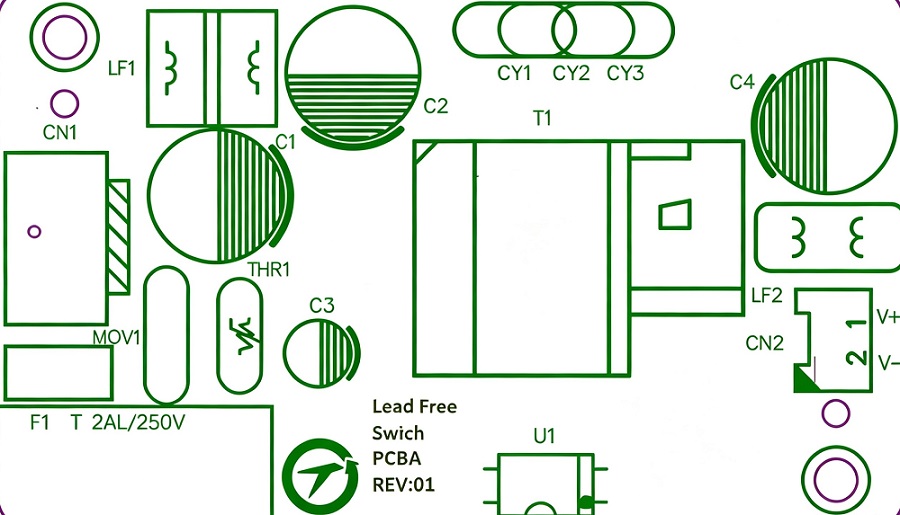
Modern engineering standards dictate that a comprehensive silkscreen carries a wealth of vital information necessary for efficient production and safe operation. Among the most critical elements are component reference designators, such as U1 for integrated circuits, R10 for resistors, and C3 for capacitors, which correspond directly to the bill of materials (BOM) and schematic diagrams. In addition to these placement guides, the legend contains component boundary outlines, pin-1 indicators for polarized ICs or diodes, and precise test point markers that assist technicians during electrical testing. Moving beyond basic assembly, the silkscreen also accommodates traceability and compliance data, including manufacturer logos, unique serial numbers, production batch codes, date codes, version numbers, and regulatory certification marks such as CE, RoHS, or Lead-Free symbols. For high-voltage or hazardous circuits, warning icons and explicit caution messages are printed to safeguard operators and end-users against accidental electrical shocks or mishandling.
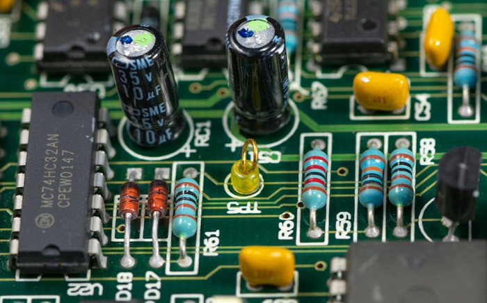
Categorizing these diverse informational elements helps engineers optimize board layouts based on specific application scenarios. Generally, silkscreen markings fall into three distinct functional categories: character silkscreen, identification silkscreen, and functional indication silkscreen. Character silkscreen focuses heavily on assembly and maintenance guidance, detailing component designators, values, and polarities to prevent manual misplacement during surface mount technology (SMT) placement and to expedite fault isolation during debugging. Identification silkscreen centers around traceability, corporate branding, and compliance management, ensuring that every manufactured unit can be tracked across its entire lifecycle while meeting regulatory mandates. Finally, functional indication silkscreen is dedicated to user interaction and safety, providing clear signifiers near connectors, switches, test points, and high-voltage zones to minimize human error and enhance overall equipment usability.
Achieving high readability and durability on the physical board requires strict adherence to engineering design rules and manufacturing constraints. The layout phase demands careful attention to size, font selection, and spatial clearance. Industry best practices recommend a minimum character height of 0.8 millimeters, with 1.0 millimeters or greater preferred for high-density boards, alongside a stroke line width of at least 0.15 millimeters. Designers should prioritize clean sans-serif typefaces like Arial to maximize legibility, ensuring uniform scaling and consistent reading orientation across the board—typically oriented from left to right and bottom to top. Furthermore, engineers must rigorously enforce spatial clearance principles: silkscreen markings must never overlap with copper pads, plated through-holes, or test points, as doing so can compromise solder paste deposition or lead to weak solder joints. A safe clearance buffer of at least 0.2 millimeters between silkscreen edges and pads is standard, expanded further in high-frequency or high-density zones. Layout optimization also requires anticipating physical blockages caused by tall components, such as electrolytic capacitors or massive aluminum heat sinks, ensuring that critical labels remain visible after assembly. For ultra-dense packaging like Ball Grid Array (BGA) components, alternative marking strategies such as diagonal slash lines or outer ring markers are frequently employed to maintain precise alignment reference.
When moving from digital computer-aided design (CAD) files to physical production, manufacturers choose among three primary fabrication methods, each balancing cost, precision, and efficiency. The first and most traditional method is conventional screen printing. As a cost-effective and straightforward technique, it utilizes epoxy inks pushed through a fine mesh screen onto the laminate surface before being thermally cured. While highly economical for large batch runs with relaxed tolerances, traditional screen printing requires larger spacing between features and extended drying times. The second method, Liquid Photo Imaging (LPI), mirrors the application process used for solder masks. A liquid photo-curable epoxy resin is coated uniformly across the board, exposed to ultraviolet light through a photographic film, and subsequently developed and cured. LPI offers significantly sharper resolution and finer line definitions compared to traditional screen printing, making it a robust middle-ground solution for modern commercial electronics. The third and most advanced technique is Direct Legend Printing (DLP), often referred to as direct inkjet printing. DLP utilizes specialized inkjet projectors combined with acrylic inks driven straight from CAD data onto the raw PCB, with ultraviolet curing occurring instantly during deposition. Although it represents the highest capital and operational cost, DLP delivers unmatched accuracy, exceptional time efficiency, and the ability to reproduce extremely fine text heights down to 0.02 inches. However, engineers must note specific material quirks, such as the fact that certain acrylic inks fail to cure properly on boards featuring silver surface finishes.
The cumulative impact of rigorous silkscreen engineering directly translates into tangible economic and operational value across the entire product lifecycle. Incorporating clear, professionally structured text and markings significantly enhances Design for Manufacturing (DFM) compliance, boosting assembly line efficiency by over thirty percent while slashing error rates and costly manual rework. During post-production maintenance, an intuitive identification system provides technicians with immediate, unambiguous visual clues, radically shrinking troubleshooting duration and elevating end-user satisfaction. Beyond functional mechanics, clean and well-balanced silkscreen typography reflects a high level of engineering discipline and corporate professionalism, instilling immediate confidence in clients and stakeholders regarding the overall quality of the electronic hardware.
Deep-Dive into the Evolution of Legend Layers
To truly master board layout optimization, one must examine how legend layers have evolved alongside automated manufacturing technologies. In the early days of electronics fabrication, manual stenciling and hand-drawn layouts dominated the workshop floor. Technicians relied on rudimentary templates to paint identification codes onto phenolic and epoxy paper substrates. As circuit densities surged with the advent of surface-mount technology (SMT), manual methods quickly proved inadequate. The miniaturization of components demanded hyper-precise application techniques, pushing manufacturers toward automated photochemical and digital inkjet solutions. Today, understanding the interplay between computer-aided design layout rules and physical printing constraints is a hallmark of elite hardware engineering.
Design Considerations for High-Density Interconnect (HDI) Boards
High-Density Interconnect (HDI) designs present unique challenges for layout engineers. With microvias, blind vias, and buried vias populating every square millimeter of available space, finding adequate real estate for text and symbols becomes exceptionally difficult. In these dense environments, standard character sizing rules often must be adapted. Engineers frequently employ micro-fonts or strategic abbreviations, ensuring that reference designators remain legible without encroaching upon critical high-speed signal traces or annular rings. Furthermore, automated optical inspection (AOI) systems utilized during modern quality control checks rely heavily on legend clarity to verify component presence and orientation, making high-precision fabrication methods mandatory for complex multilayer assemblies.
Evaluating Ink Chemistry and Environmental Durability
The chemical composition of the ink utilized during fabrication directly dictates the longevity and environmental resilience of the final product. Epoxies used in traditional screen printing offer robust chemical resistance, making them ideal for industrial and automotive environments exposed to harsh solvents and fluctuating temperatures. Conversely, acrylic inks utilized in direct legend printing provide rapid UV-curing cycles but require careful evaluation when dealing with specific surface platings, such as immersion silver or electroless nickel immersion gold (ENIG). Ensuring optimal adhesion between the solder mask and the ink layer prevents flaking, peeling, or fading over years of field operation, thereby protecting brand reputation and reducing field failure rates.
Streamlining Quality Control and Inspection Protocols
Quality assurance teams depend extensively on legible markings to streamline inspection protocols and accelerate throughput. When inspecting batches of complex circuit boards, inspectors must quickly cross-reference physical components against assembly drawings. Clear, uniform typography eliminates ambiguity, preventing costly assembly line stoppages and ensuring that regulatory compliance marks remain visible and scannable. By integrating rigorous design rules early in the layout phase, engineering teams foster a seamless bridge between digital schematics and physical hardware realization, ultimately driving down overall production costs.
The Impact of Silkscreen Quality on Automated Optical Inspection (AOI)
Automated Optical Inspection (AOI) systems are the backbone of modern electronics manufacturing, tasked with identifying soldering defects, missing components, and tombstoning errors at lightning speeds. These optical machines rely heavily on high-contrast legend markings to anchor their coordinate systems and verify component placement accuracy. If a legend is blurred, smudged, or improperly aligned due to poor printing resolution or inferior ink selection, AOI algorithms may trigger false positives or miss critical assembly flaws entirely. Consequently, investing in advanced printing technologies directly enhances factory floor throughput and reduces unnecessary manual inspection overhead.
Addressing Thermal Stress and Environmental Aging in Harsh Environments
Electronic hardware deployed in aerospace, automotive, and industrial automation environments is constantly subjected to extreme thermal cycling, mechanical vibration, and corrosive airborne agents. Under such rigorous conditions, subpar legend inks can degrade, yellow, or delaminate from the underlying solder mask. Selecting robust epoxy or specialized UV-curable formulations ensures that essential safety warnings, voltage ratings, and part numbers remain legible throughout the entire operational lifecycle of the equipment. This durability is not merely an aesthetic preference; it is a critical safety requirement that ensures technicians can safely service and troubleshoot hardware years after initial deployment.
In summary, treating the legend layer as an afterthought can introduce severe bottlenecks into production, whereas treating it as a core engineering discipline safeguards manufacturing flow from fabrication to final deployment. By balancing meticulous design rules, selecting the most appropriate production methodology, and organizing information logically, hardware engineering teams can transform a simple layer of ink into a powerful catalyst for efficiency, compliance, and product excellence. Whether you are designing a high-speed telecommunications motherboard or a compact consumer gadget, investing time into refining your printed circuit board silkscreen layout pays dividends every single time a board rolls off the assembly line.