A Trustworthy PCB and Electronic Manufacturing Enterprise! Contact Us



Circuit board shielding plays an important role in reducing electromagnetic interference and protecting sensitive electronic circuits. As electronic products become smaller and more connected, engineers are paying more attention to how different circuits interact with each other inside the same enclosure.A modern electronic product may contain a processor, wireless module, sensors, power conversion circuits, memory, communication interfaces, and other components on a relatively small PCB. Each section can generate or receive electromagnetic energy. When these circuits are placed too close together, unwanted coupling can affect signal quality, product stability, and even compliance testing.For this reason, shielding is no longer limited to specialized RF equipment. It can also be found in wireless devices, industrial controllers, automotive electronics, medical equipment, communication systems, and many other products.
Why Electromagnetic Interference Matters
Electromagnetic interference, commonly known as EMI, occurs when unwanted electrical or electromagnetic energy affects another circuit.The source can be inside the same PCB or somewhere else in the product. A switching regulator, processor, motor driver, wireless transmitter, or high-speed interface can all generate unwanted noise.
The problem is that interference does not always show up immediately during development.A prototype may work normally on an engineer's desk, but the behavior can change when the PCB is installed inside its final enclosure. Cables are connected, other modules are powered, and the product begins operating under real conditions. Suddenly, a wireless connection becomes unstable, a sensor produces unexpected readings, or a communication interface starts losing data.
These problems can be difficult to solve late in development.Shielding is one of the methods engineers can use to control this type of problem. It creates a conductive barrier around a sensitive or noisy circuit, helping reduce unwanted electromagnetic coupling between different areas.However, shielding should not be viewed as a replacement for good PCB layout. Grounding, routing, stackup design, component placement, and return-current paths all have a direct influence on the final result.
How PCB Shielding Works
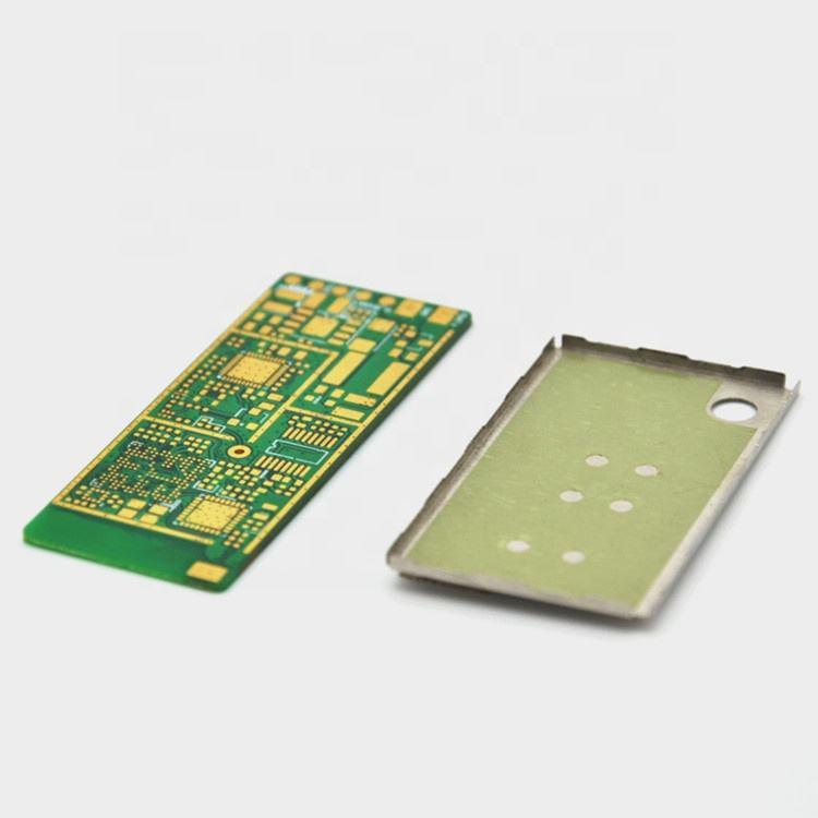
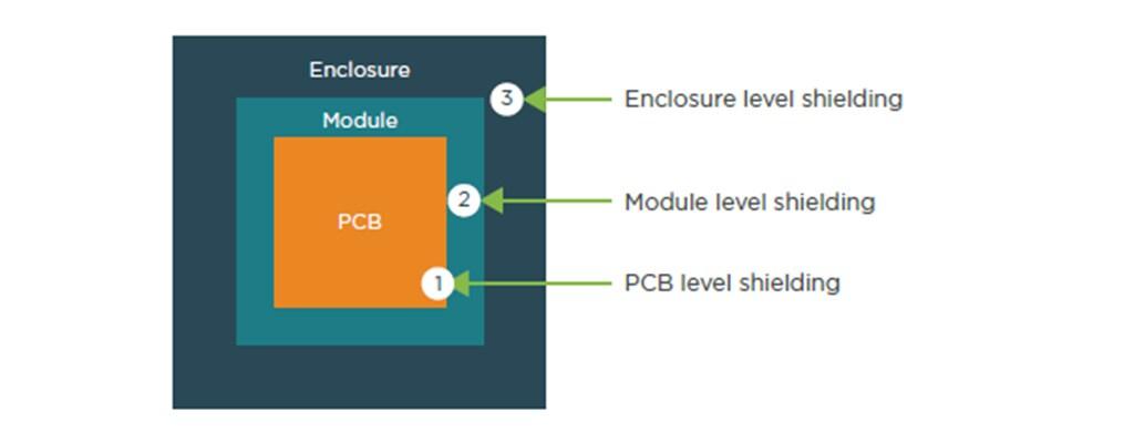
The basic idea is straightforward.A conductive structure is placed around a circuit or component that needs protection. The structure is normally connected to ground so that unwanted electromagnetic energy can be controlled or redirected.In practical PCB designs, the shielding structure may take several forms.A metal shielding can is one common solution. A frame is soldered to the PCB, and a metal cover is installed over the protected area. This approach is especially common around RF modules and wireless communication circuits.Another approach is to use grounded copper areas and via structures. A continuous ground plane can provide a low-impedance return path, while a row of ground vias can create a boundary around a sensitive circuit.The correct solution depends on the frequency range, circuit architecture, mechanical structure, available PCB space, and production requirements.There is no universal shielding method that works equally well for every electronic product.
Common Shielding Methods
Metal Shielding Cans
Metal cans are widely used in consumer electronics, communication equipment, GPS devices, wireless modules, and RF products.A typical structure consists of a soldered frame and a removable or fixed cover. The frame creates an electrical boundary around the circuit.One advantage is that the shield can be designed around a specific functional block instead of covering the entire PCB.For example, a product may have a Bluetooth module, a power supply section, and a digital processor on the same board. It may not be necessary to shield all three areas. The RF section may receive the greatest benefit from a dedicated shield.This can reduce material cost and simplify the mechanical design.
Ground Planes
Ground planes are a basic but important part of PCB design.A well-designed reference plane provides a controlled return path for signals and can reduce unwanted coupling. In high-speed and RF designs, maintaining a continuous reference plane is particularly important.However, simply filling an unused area with copper does not automatically solve EMI problems.The designer still needs to consider where current flows, where return paths are located, and whether high-speed traces cross gaps or discontinuities in the reference plane.
Via Fences
A via fence consists of multiple vias connected to ground and placed around a PCB area.Via fences are frequently used in RF and microwave circuits. They can help contain electromagnetic fields and provide better isolation between different sections of a board.The spacing between vias is important. The appropriate spacing depends on the operating frequency and the physical structure of the PCB.At higher frequencies, dimensions that appear very small from a mechanical perspective can have an electrical effect. This is why RF PCB layout requires more attention to geometry than a conventional low-speed control board.
Conductive Enclosures
Some products use a conductive metal enclosure around the complete electronics assembly.This approach can provide a higher level of electromagnetic protection, but it also introduces mechanical and thermal considerations.Connectors, cables, ventilation openings, seams, and mounting points can all affect the final shielding performance.In other words, even a well-shielded PCB may not perform as expected if the surrounding product structure provides an easy path for interference.
Shielding and PCB Layout
Good layout is often the first line of defense.Sensitive circuits should be kept away from noisy circuits whenever possible. RF traces should be short and routed with appropriate reference planes. High-speed differential pairs should follow their intended impedance-controlled paths.Power conversion circuits also deserve special attention.Switching regulators contain fast voltage and current transitions. If a noisy switching node is placed next to a sensitive analog input or RF circuit, the resulting coupling may be difficult to eliminate later.Component placement therefore matters just as much as the shield itself.A common mistake is to finish the PCB layout first and then try to add a shield around whatever section appears to have an interference problem. Sometimes this works, but in other cases the shield footprint conflicts with components, connectors, mounting holes, or thermal structures.It is usually easier to reserve the required space during the original layout.
High-Frequency PCB Applications
RF and high-frequency products are particularly sensitive to electromagnetic coupling.A wireless communication circuit may contain a transmitter and receiver operating at several gigahertz. Radar equipment can operate at even higher frequencies. At these frequencies, PCB geometry becomes part of the electrical design.Trace length, dielectric thickness, copper geometry, via position, grounding, and material selection can all influence signal behavior.For this reason, shielding should be considered together with the PCB stackup.A designer working on an RF product may require a specific laminate, controlled impedance, defined dielectric thickness, low-loss material, and carefully controlled copper features.A shielding solution that works well on a standard FR-4 control board may not produce the same result on a high-frequency RF design.This is also where communication between the design team and PCB manufacturer becomes useful. Manufacturing engineers can review whether the proposed stackup, trace geometry, vias, clearances, and material specifications can be produced consistently.
Shielding in High-Speed Digital Designs
Shielding is not only an RF topic.Modern digital interfaces can have very fast signal transitions. Even when the nominal data rate does not appear extremely high, fast edge rates can contain significant high-frequency components.USB, PCIe, Ethernet, display interfaces, memory buses, and other high-speed systems may require careful attention to signal integrity and electromagnetic compatibility.In these designs, routing and return paths are usually the starting point.A signal trace should have an appropriate reference plane. Avoiding unnecessary discontinuities helps control impedance and reduce unwanted radiation.If a particularly sensitive circuit is located next to a noisy interface, physical separation and grounding can be combined with shielding to improve isolation.
Thermal Problems Behind a Shield
One detail that is sometimes overlooked is heat.A metal shield can improve electromagnetic isolation, but it can also reduce airflow around components.This may become an issue when the shield covers a power amplifier, processor, voltage regulator, or another component that generates significant heat.Engineers should therefore check the thermal behavior before finalizing the shield structure.In some designs, the shield can be connected to a thermal path or designed with a suitable mechanical interface. In others, the component may need to be moved outside the shielded area.Ventilation openings are another possible solution, but they need to be evaluated carefully because openings can affect electromagnetic performance.The best design is usually a compromise between electrical, thermal, mechanical, and manufacturing requirements.
Shielding and PCBA Assembly
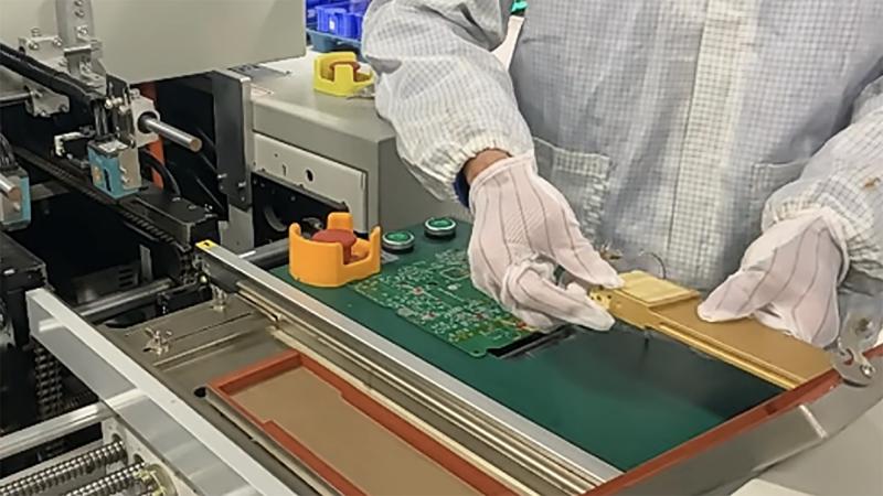
The electrical design is only part of the equation.When the PCB moves into PCBA production, the shielding structure needs to work with the assembly process.For a shield frame installed through SMT, the PCB footprint needs suitable soldering areas and clearances. The manufacturing line also needs to accommodate the shield structure.For low-volume prototypes, manual assembly may be acceptable. Once production volume increases, however, manual operations can become expensive and introduce additional variation.This is why engineers should consider the production method at an early stage.A design that is easy to assemble repeatedly is generally easier to scale.Inspection is another consideration. A permanent metal cover can make visual inspection and troubleshooting more difficult. A removable shield may cost slightly more but provide better access during service.The right choice depends on the product and expected production process.
DFM Considerations
Design for manufacturability is particularly useful when a PCB contains shielding structures.Before manufacturing, engineers can review the shield footprint, copper clearances, solder mask openings, grounding points, component heights, and mechanical dimensions.For RF boards, the review can also include controlled impedance, material selection, stackup configuration, and via structures.This kind of review is most useful before the Gerber files are finalized.Changing a shield footprint at the prototype stage is usually much easier than changing it after tooling and production have already started.For companies developing a new hardware product, early communication with the PCB manufacturer can therefore save both time and engineering effort.
Testing the Shielding Design
A shield should be tested rather than assumed to work.Depending on the product, testing may include conducted emissions, radiated emissions, RF performance, susceptibility, or functional testing.If interference is found, the solution is not always to make the shield larger.The root cause may be poor grounding, an incorrect return path, a noisy power circuit, a routing problem, or an opening in the mechanical enclosure.Engineers can compare different configurations during testing to identify where the problem is actually coming from.This approach is more effective than making several changes at the same time and then trying to determine which one helped.
Balancing Performance and Cost
Adding more shielding does not automatically mean better product design.Every additional shield adds material, assembly requirements, and potentially more mechanical complexity.For a high-volume consumer product, even a small increase in per-unit cost can become significant.A better approach is to identify the circuits that genuinely need isolation.For example, a sensitive receiver may require a dedicated shield while a basic digital control section does not.This selective approach can provide the required protection without turning the entire PCB into a complicated mechanical structure.
Choosing a PCB Manufacturing Partner
For projects involving RF, high-speed signals, or sensitive analog circuits, the manufacturing partner can influence the final result.The manufacturer should understand the relationship between PCB materials, stackup, impedance, copper geometry, via structures, and assembly requirements.At iPCB, we support PCB and PCBA projects ranging from standard multilayer boards to high-frequency and high-speed applications. DFM review can be included early in the process to identify potential manufacturing issues before production.For engineers, this can be particularly useful when a project includes controlled impedance, RF sections, fine-pitch components, or specialized materials.A practical manufacturing discussion does not need to wait until the final Gerber files are released. Earlier communication can make the transition from prototype to production much smoother.
Final Thoughts
Good shielding is rarely achieved by adding a metal cover at the end of a PCB project.It starts with component placement, routing, grounding, stackup design, material selection, and mechanical planning. The shield is then used as one part of the overall electromagnetic design.For wireless, RF, high-speed, industrial, and sensitive electronic products, this approach can help engineers reduce interference problems before they become expensive redesigns.The most effective design is usually not the one with the most shielding. It is the one where the PCB layout, grounding, materials, mechanical structure, and manufacturing process have been considered together from the beginning.