A Trustworthy PCB and Electronic Manufacturing Enterprise! Contact Us



Large PCB manufacturing requires more than simply producing a circuit board with greater dimensions. As board size increases, factors such as material stability, copper distribution, warpage, signal integrity, thermal management, and assembly can have a greater influence on the final result. Large boards are commonly used in industrial automation, power electronics, communication equipment, transportation systems, and other applications where a compact PCB cannot provide enough space for all the required circuits and connectors.
Why Large PCB Design Requires More Attention
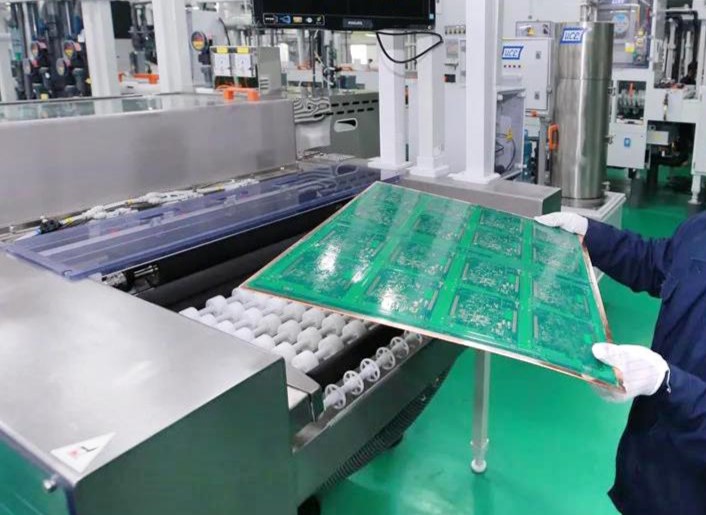
A PCB may look straightforward in a CAD program, but its physical behavior can become more complicated as its dimensions increase. During fabrication, the board goes through processes such as lamination, drilling, copper plating, etching, soldering, and reflow. These processes expose the PCB to heat and mechanical stress. Materials expand and contract as temperatures change, and even a small amount of dimensional movement can become more noticeable across a larger surface.
This can affect connector alignment, mounting holes, layer registration, and overall board flatness. A design that works perfectly well on a small board may therefore require additional engineering consideration when the same basic structure is expanded. For manufacturers, the question is not only whether a board can physically be produced, but whether it can be produced repeatedly within the required tolerances.
Material Selection and Board Stability
Material selection is an important part of large PCB design. Standard FR-4 is suitable for many industrial and electronic applications, but the best material depends on the electrical, thermal, and mechanical requirements of the project. High-speed or RF designs may require low-loss materials, while power electronics may place greater emphasis on thermal performance and copper thickness.
The laminate structure also influences dimensional stability. A large multilayer board contains several layers of copper and dielectric materials, and each material responds differently to temperature and mechanical stress. A well-balanced stackup can help reduce unwanted deformation and make the finished board more predictable during manufacturing. For this reason, the stackup should be reviewed together with the board dimensions rather than treated as a separate electrical specification.
Managing Warpage on Large Boards
Warpage is one of the most common manufacturing concerns when board dimensions become larger. A PCB can experience deformation because of differences in copper distribution, laminate construction, thermal exposure, and internal stress. The problem may become particularly noticeable during SMT assembly, when a large or relatively thin board needs to remain stable while passing through production equipment.
Copper balance is one factor that can help. If one area of the board contains a large amount of copper while another area contains very little, the structure may experience uneven stress during processing. A suitable layer arrangement, balanced copper distribution, and appropriate board thickness can all contribute to better stability. These details are easier to address during the design stage than after production has already started.
Copper Weight and Power Requirements
Many large PCBs are used in industrial or power-related applications, so copper thickness can become an important consideration. Heavier copper can provide advantages for high-current applications and heat distribution, but it also changes the manufacturing process. Etching, plating, drilling, and fine-line formation can become more demanding when copper thickness increases.
The right copper weight should therefore be based on actual current, thermal, and electrical requirements rather than simply selecting the heaviest option available. A design that combines heavy copper with fine traces or high-density features may need additional manufacturing evaluation. Discussing these requirements with the PCB manufacturer before finalizing the design can help avoid unnecessary limitations later.
Signal Integrity on Larger Boards
Board size itself does not determine whether a design is high-speed, but many large boards contain long signal paths and several different functional sections. A single board may include processors, sensors, communication interfaces, power circuits, and external connectors. When these sections are spread across a large area, routing and return paths need to be considered carefully.
For high-speed signals, controlled impedance and continuous reference planes remain important. Differential pairs should be routed according to the requirements of the interface, while unnecessary changes in routing structure should be avoided. If the design includes RF or high-frequency circuits, material selection, dielectric thickness, trace geometry, and grounding become even more important. A larger board therefore benefits from close cooperation between the layout engineer and the PCB manufacturer, especially when specific impedance or high-frequency materials are involved.
Mechanical Design Matters Too
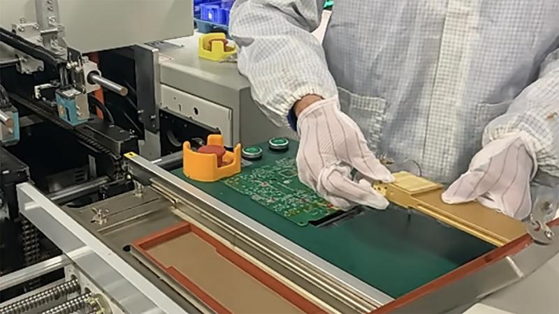
A large PCB is also a mechanical component, particularly when it is installed inside industrial equipment. Mounting points, connectors, enclosure dimensions, component height, and board support should be considered during the layout stage. Heavy components such as large connectors, transformers, heatsinks, or power components can create additional mechanical stress if they are positioned far from suitable support points.
The board also needs to fit correctly inside the final product. A few millimeters of difference in a mounting hole or connector position can become a real problem when the PCB has to align with an enclosure or external interface. For this reason, mechanical and electrical design should not be treated as completely separate tasks when developing a large board.
Panelization and Manufacturing Cost
The physical size of a PCB can also affect production cost because it changes how efficiently the board can be arranged on a manufacturing panel. Smaller boards can often be produced several at a time, while a large-format board may occupy most of the available panel area. This directly affects material utilization and production efficiency.
However, board size is only one part of the quotation. Layer count, material, copper weight, surface finish, drilling requirements, tolerances, order quantity, and panel utilization can all influence the final price. In some cases, a small change to the board outline or production arrangement can improve panel efficiency. This is why it is useful to discuss the manufacturing approach before the design is completely fixed.
Prototyping Before Mass Production
For a large PCB, prototyping should cover both electrical and mechanical performance. Engineers can use the first prototype to confirm that the board fits correctly inside the enclosure, connectors align with their intended positions, mounting holes are accurate, and the board remains sufficiently stable after assembly. Thermal behavior and signal performance can also be evaluated under realistic operating conditions.
These checks are particularly valuable for industrial products because a PCB may need to operate continuously for many years. Finding a mechanical or manufacturing issue during prototyping is much easier to handle than discovering the same problem after a large production run. A prototype therefore provides more than functional verification; it also gives the manufacturer and engineering team an opportunity to confirm that the design is practical for repeatable production.
DFM Review Before Production
Design for manufacturability can be especially useful for large-format boards. Before fabrication, the manufacturer can review board dimensions, layer structure, copper distribution, minimum trace and spacing, hole sizes, mounting holes, edge clearance, impedance requirements, and other production details. The purpose is not to change the engineer's design unnecessarily, but to identify potential manufacturing problems while changes are still relatively easy to make.
For example, a mounting hole may need additional clearance, a copper area may need better balance, or a particular via structure may require a different production method. These adjustments can often be handled during the engineering review without affecting the main function of the product. Early DFM communication can therefore reduce unnecessary prototype iterations and make the transition into volume production smoother.
From Prototype to Volume Production
A board that works during prototyping still needs to be evaluated from a production perspective before moving into volume manufacturing. Prototype production can involve more manual inspection and engineering attention, while mass production requires stable processes, consistent materials, predictable yield, and efficient assembly.
This becomes particularly important for a large PCB because material handling, board support, inspection, and assembly equipment may all be affected by the physical dimensions. A pilot production run can provide useful information about these factors before a larger order is released. It allows the engineering team to confirm that the production process can deliver consistent results rather than relying only on the performance of a few prototype boards.
Working With an Experienced PCB Manufacturer
For complex PCB projects, involving the manufacturer early can make the development process more efficient. Engineers do not always need to wait until the final Gerber files are completed before starting a manufacturing discussion. Basic information such as board dimensions, layer count, material, copper requirements, estimated quantity, and application can already provide a useful starting point for feasibility analysis.
At iPCB, we support PCB and PCBA projects covering multilayer, industrial, high-speed, RF, and other specialized applications. Our engineering team can review manufacturing requirements such as stackup, material selection, impedance, copper distribution, drilling, and assembly conditions before production. For a large-format board, this type of early review can help identify practical manufacturing considerations before they become costly changes.
Final Thoughts
Large PCB projects are not simply smaller circuit boards made bigger. As the physical dimensions increase, mechanical stability, material behavior, copper distribution, thermal management, signal integrity, assembly, and production efficiency become more closely connected. A successful design needs to work not only electrically, but also during fabrication, assembly, installation, and long-term operation.
The best approach is to consider manufacturing requirements while the design is still flexible. With suitable materials, a balanced stackup, practical mechanical design, appropriate copper distribution, and early DFM communication, a large-format PCB can be made more predictable and easier to scale from prototype to volume production.