A Trustworthy PCB and Electronic Manufacturing Enterprise! Contact Us



A high‑quality strong green pcb board strong has become a go‑to choice for modern electronic manufacturing, as the global electronics industry shifts toward eco‑friendly production and low‑carbon operations. Today, more brands, engineers, and procurement teams are ditching traditional circuit boards with harmful chemical components and choosing sustainable alternatives to meet international environmental standards.
Many people mistakenly believe eco‑friendly circuit hardware is defined only by solder mask colour, but real sustainability comes from material composition and manufacturing workflows. To understand why green PCB solutions are gaining popularity, we first need to look at the problems caused by conventional printed circuit boards. Traditional PCBs widely use halogen‑based flame retardants, lead‑containing surface finishes, and non‑recyclable epoxy resins. When these boards are scrapped, buried, or incinerated, they release toxic substances that pollute soil and groundwater. For decades, electronic waste has been one of the hardest waste categories to process, largely due to harmful PCB materials. As global regulations like RoHS, REACH, and WEEE become stricter, ordinary circuit boards can no longer meet export and environmental compliance requirements. This is why more manufacturers are upgrading their production lines and adopting strong halogen‑free PCB assemblies strong to replace outdated, high‑pollution circuit solutions.
It is important to correct the most common industry misunderstanding: board colour does not define sustainability. Many beginners assume any PCB with green solder mask is an eco‑friendly product, which is completely wrong. Green solder mask was mainstream in the past because it offers good visual inspection contrast, stable UV resistance, and low production cost. Manufacturers can now produce blue, black, white, and red solder masks with ordinary non‑environmental materials. Real sustainable performance relies on raw material selection and fabrication standards. Designers and buyers should prioritise strong RoHS compliant printed circuit boards strong when sourcing hardware for global‑targeted electronic devices. It uses halogen‑free substrates, lead‑free surface treatments, low‑carbon manufacturing procedures, and low‑toxicity auxiliary materials. Every production link is optimized to reduce chemical residue, waste emissions, and environmental damage, while ensuring the circuit’s electrical stability and safety remain unchanged.
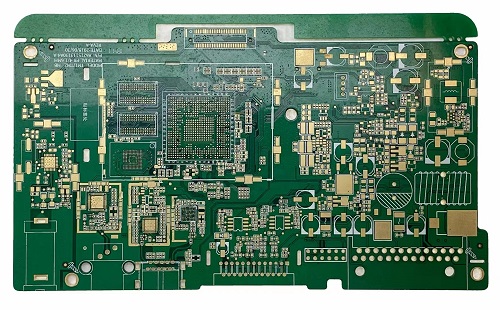
Material optimization is the core advantage of sustainable green PCBs. Most traditional FR4 substrates rely on brominated halogen flame retardants to achieve fire resistance. Although effective, these substances produce harmful dioxins during high‑temperature combustion, posing serious threats to the ecological environment. Modern eco‑friendly circuit boards use upgraded halogen‑free FR4 materials with phosphorus and nitrogen‑based flame retardants. These alternatives deliver the same UL94‑V0 fireproof rating but produce almost no toxic substances after disposal. In addition, qualified green boards adopt lead‑free surface finishes such as OSP, immersion silver, and lead‑free tin plating, completely eliminating lead pollution during production and recycling. For electronic products that require long‑term outdoor use or high‑frequency operation, these upgraded materials also improve high‑temperature resistance, anti‑aging performance, and overall equipment stability. A well‑specified green pcb board will keep consistent performance even under continuous temperature cycling, a key advantage for industrial‑grade hardware.
Beyond material improvements, standardized production processes further enhance the practical value of green circuit boards. Traditional PCB manufacturing involves large amounts of chemical etching, cleaning, and surface treatment, generating substantial wastewater and chemical waste. Regular factories often discharge untreated waste, causing long‑term environmental harm. Professional manufacturers that produce eco‑friendly PCBs apply closed‑loop water circulation systems, copper recovery technology, and neutralized waste discharge processes. They optimize board layout to reduce substrate scrap and use renewable energy to lower carbon emissions. Compared with ordinary boards produced through traditional processes, professionally manufactured eco‑friendly circuits effectively reduce the product’s full‑life carbon footprint, helping brands meet ESG assessment requirements and green factory certification standards.
The application scope of eco‑friendly PCBs continues to expand across almost all mainstream electronic industries. Consumer electronics is the largest application field. Smart home devices, wearable gadgets, wireless earphones, and household sensors are updated quickly and produce massive e‑waste every year. European and American markets have strict access thresholds for such products, forcing brands to fully adopt environmentally friendly circuit materials. If products fail green compliance tests, they will face export restrictions and market recalls.
The new energy and automotive electronics industries also rely heavily on sustainable PCB solutions. New energy vehicles, solar inverters, and energy storage equipment have long service cycles and high operational stability requirements. These devices work in complex environments with alternating high and low temperatures, vibration, and humidity. Ordinary PCBs are prone to aging, delamination, and circuit failure, while halogen‑free substrates offer better thermal stability and corrosion resistance. At the same time, new energy products emphasize environmental protection and recyclability, making low‑toxicity circuit materials a basic industry standard.
Industrial automation and medical electronics are also accelerating the adoption of green circuit technology. Industrial control equipment runs continuously throughout the year and requires extremely high circuit reliability. Eco‑friendly boards with stable material properties effectively reduce failure rates and extend equipment service life. Medical devices have stricter safety standards; low‑toxicity and pollution‑free circuit materials avoid chemical precipitation that may affect equipment accuracy and user safety. In high‑precision equipment scenarios, the comprehensive performance advantages of green PCBs far outweigh their slight cost differences.
Many buyers and designers hesitate to choose green PCBs due to the misconception that eco‑friendly boards are expensive and reduce product performance. In fact, after years of technological iteration and large‑scale mass production, the cost gap between green and ordinary PCBs has narrowed sharply. For medium and large batch orders, the price difference is almost negligible. In terms of performance, modern halogen‑free substrates have surpassed traditional materials in high‑temperature resistance, insulation stability, and anti‑interference ability. The only minor limitation is that ultra‑low‑cost prototype small‑batch orders may have slightly higher unit prices, which is completely acceptable for formal commercial product development.
To maximize the value of green circuit boards, designers need to master scientific selection and design methods. First, select matched substrate materials according to product application scenarios. Civilian ordinary products can use conventional halogen‑free FR4, while high‑temperature and high‑frequency equipment needs upgraded high‑reliability green substrates. Second, choose reasonable surface finishes: OSP is cost‑effective and environmentally friendly for ordinary SMD boards, while ENIG and immersion silver are suitable for high‑precision, long‑life products. Third, optimize circuit layout to reduce board area waste and improve material utilization, further reducing comprehensive production costs.
It is also necessary to avoid common procurement pitfalls when purchasing green PCBs. Some unscrupulous suppliers falsely label ordinary green solder mask boards as eco‑friendly products without real halogen‑free and low‑toxicity certifications. Buyers must ask suppliers for complete test reports including RoHS, halogen‑free certification, and environmental factory audit documents. In addition, users should not only focus on the bare board materials but also check the environmental compliance of supporting electronic components, solder paste, and auxiliary materials to ensure the entire product meets green standards.
Looking ahead, green and low‑carbon development will become the core trend of the global electronics manufacturing industry. With the continuous improvement of e‑waste recycling systems and the maturity of bio‑based resin materials, future circuit hardware will achieve higher recyclability, lower costs, and stronger performance. Traditional high‑pollution PCB products will gradually be phased out of the mainstream market. For electronic enterprises and design engineers, actively adapting to green manufacturing trends and mastering the application skills of eco‑friendly circuit boards is key to enhancing product market competitiveness and meeting global environmental access standards. In short, the green pcb board is not a superficial environmental marketing concept, but a practical, high‑performance, and sustainable circuit solution that supports electronics brands to balance product reliability and global environmental regulatory requirements.