A Trustworthy PCB and Electronic Manufacturing Enterprise! Contact Us



In the early stage of PCB design, both engineers and purchasers often face a common dilemma: whether to select a 2-layer, 4-layer, or 6-layer PCB. Most selections rely on past experience. Some teams choose fewer layers simply to cut costs, resulting in poor signal stability and failed EMC tests. Others over-design with extra multilayer layers, unnecessarily raising production costs and extending lead times. In fact, there is no one-size-fits-all formula for PCB layer selection. The core is to find the best balance among circuit complexity, signal integrity, EMC performance and mass production cost. Based on practical manufacturing experience, this article systematically explains how to select the most suitable PCB layer count for different projects, avoiding design rework and unnecessary cost waste.
The fundamental selection principle is clear: more PCB layers allow independent segmentation of signal layers, power layers, and ground layers. This provides more routing space, complete signal return paths, and better electromagnetic shielding, effectively improving product stability and EMC compliance. However, more layers also mean higher material costs, more complex lamination processes, and longer production lead times. Conversely, fewer layers reduce costs and accelerate production, but come with limited routing space and incomplete ground planes. These drawbacks amplify high-frequency crosstalk, power ripple, and electromagnetic interference. All PCB layer selections follow this core logic.
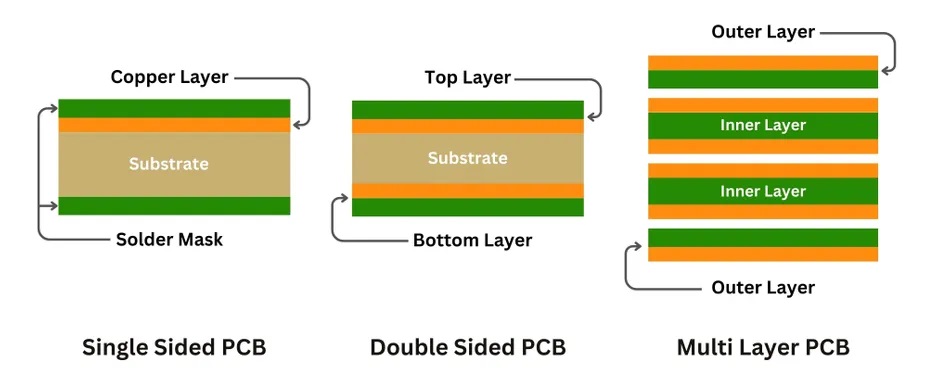
As the most basic PCB structure, a 2-layer PCB consists only of top and bottom signal layers without inner plane layers. Its application scenarios are highly specific. The key advantages of 2-layer PCBs are ultra-low cost, simple manufacturing process and short lead time. They are ideal for low-frequency, low-voltage and simple circuits, including ordinary household appliance control boards, toy circuits, basic switching power supplies, and low-speed industrial control modules. For these low-demand projects with limited traces and no strict impedance control or EMC shielding requirements, 2-layer PCBs are fully competent.
Nevertheless, 2-layer PCBs have obvious limitations. Without independent ground and power inner layers, power and ground traces have to be routed on the same planes as signal traces. This easily causes excessive signal return loop areas, power noise coupling, and crosstalk between high-speed and low-speed signals. Such structures cannot support high-frequency circuits, precision analog circuits, or high-speed interface circuits. Projects involving clock signals, differential pairs, RF transmission, and low-voltage high-current circuits often suffer from unstable operation and EMI over-limit issues if forcibly designed with 2-layer PCBs.
The 4-layer PCB is currently the most cost-effective option widely adopted in consumer electronics and industrial products. It perfectly balances electrical performance, EMC capability and manufacturing cost. Compared with 2-layer PCBs, 4-layer designs support independent complete ground and power planes. The layered arrangement of signal, ground, and power layers effectively solves voltage drop and power ripple issues. Meanwhile, the solid ground planes optimize signal return paths, significantly reducing electromagnetic crosstalk and radiation interference to meet standard EMC certification requirements.
4-layer PCBs apply to most mid-range projects, such as IoT control boards, wearable device circuits, general industrial control motherboards, USB/serial communication circuits, and medium-low power power supply boards. For projects with a small number of high-speed signals, analog sampling circuits and low-voltage high-current circuits, 4-layer PCBs are the optimal choice. They avoid the performance shortcomings of 2-layer boards and the cost redundancy of 6-layer or 8-layer boards. In mass production, 4-layer PCBs feature excellent DFM compliance and stable production yield, making them the mainstream solution for most commercial projects.
Multilayer PCBs with 6 or more layers are high-performance solutions focused on superior signal integrity and EMC shielding, solving complex design challenges that 4-layer PCBs cannot handle. High-layer-count PCBs support isolated multiple ground planes, partitioned power planes, and hierarchical placement of high-speed and low-speed signals. They effectively eliminate crosstalk caused by plane splitting, high-frequency interference, and impedance deviation. Superimposed multi-ground planes provide comprehensive electromagnetic shielding and greatly enhance system stability and anti-interference capability.
These high-layer PCBs are exclusively suitable for sophisticated and high-end devices, including high-speed communication mainboards, RF equipment, precision instruments, industrial servo control boards, circuits with HDMI/Gigabit Ethernet interfaces, and high-density BGA-based motherboards. Such products feature dense routing, abundant high-speed signals, complex electromagnetic environments and strict EMC certification standards, which cannot be supported by 4-layer structures. It is worth noting that higher layer counts bring more complicated lamination procedures, higher material costs and longer lead times. Unnecessary layer upgrading should be avoided in conventional projects.
EMC performance is a critical factor in layer selection. For products requiring CE, FCC, 3C and other EMC certifications, especially those equipped with high-frequency clocks, switching power supplies and relay interference sources, 2-layer PCBs are not recommended. 4-layer PCBs are preferred for isolating high/low voltage and strong/weak signals through independent ground planes to suppress radiation interference. For complex high-frequency and high-density equipment, 6-layer or higher multilayer PCBs are necessary. Dual ground planes provide enhanced shielding to fundamentally eliminate EMI over-limit risks at the hardware level.
Cost optimization follows the rule of "sufficient design is optimal". Adopting 4-layer PCBs for simple low-frequency projects will increase material costs by 30% to 50%. In contrast, choosing low-cost 2-layer PCBs for high-speed precision projects leads to sharply increased debugging, rework and certification costs, and even batch product scrapping. The standardized selection principle for mass production is: 2-layer for simple low-frequency circuits, 4-layer for conventional high-speed projects, and 6-layer or above for complex and precision equipment.
In conclusion, more PCB layers do not equal better performance. The optimal layer count depends on targeted project requirements. Reasonable selection based on circuit frequency, signal precision, EMC standards and mass production costs can effectively avoid insufficient performance, electromagnetic interference and system instability. It also minimizes manufacturing expenses and improves product market competitiveness, achieving a perfect balance between technical feasibility and commercial mass production.