A Trustworthy PCB and Electronic Manufacturing Enterprise! Contact Us



Flexible circuit construction relies on the right Film Substrate to deliver electrical insulation, mechanical support and chemical shielding for copper traces and mounted components. Its intrinsic properties directly define flex circuit bendability, fold endurance, electrical performance and long‑term environmental stability. As flexible circuit requirements grow more demanding, continuous innovation of Film Substrate becomes one of the key driving forces behind flexible PCB advancement. This article walks through mainstream flexible dielectric films, compares material performance, reviews manufacturing synergy and analyzes ongoing market shifts for hardware engineers and procurement specialists working on flex‑oriented electronic projects.
1. Electronic Device Trends and the Rise of Flexible Circuits
Consumer expectations for electronic hardware keep rising in today’s digital landscape. Designers are constantly challenged to balance compact size, light weight and enhanced functionality. Traditional rigid circuit boards cannot satisfy the spatial constraints of foldable, wearable or implant‑capable hardware. Flexible printed circuits (FPC) solve these pain points by enabling bending, twisting and repeated folding without permanent damage. They replace bulky wiring harnesses inside smartphones, wearables, medical implants and automotive sensor modules. Every performance gain observed in end‑products traces back to careful material selection at the substrate level. Without well‑matched flexible dielectric materials, many novel flexible‑hardware concepts would remain unfeasible for mass production.
2. Categories and Key Properties of Flexible Film Materials
2.1 Polyimide (PI) Film
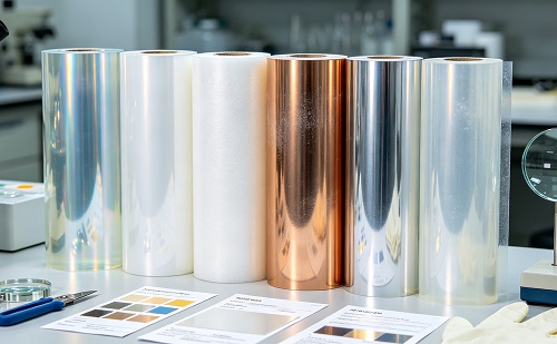
This widely‑used Film Substrate, polyimide ranks as the most widely adopted flexible dielectric material for commercial flexible circuits.Polyimide ranks as the most widely adopted flexible dielectric material for commercial flexible circuits. Its thermal decomposition temperature exceeds 500℃, allowing long‑term stable operation under high‑temperature operating conditions. For electronic sub‑systems near heat‑generating processors, PI‑based flex circuits maintain stable characteristics without performance degradation. In aerospace electronics deployed close to engine assemblies, PI reliably withstands extreme thermal cycling encountered during flight missions.
PI delivers outstanding mechanical performance, with tensile strength ranging from 150‑300MPa and elastic modulus between 3‑6GPa. Subjected to repeated bending, folding and minor stretching, PI preserves structural integrity and consistent electrical output. Foldable smartphone internal flex interconnects endure tens of thousands of folding cycles; high‑grade PI prevents trace cracking and component detachment, laying a solid reliability foundation for consumer foldable devices.
Excellent chemical resistance and dielectric insulation represent another major strength. PI tolerates common acids, alkalis and organic solvents, protecting inner copper traces against chemical corrosion. Volume insulation resistance reaches 10¹⁵‑10¹⁷Ω・cm, paired with moderate dielectric constant 3‑4 and low dissipation factor. During high‑speed signal transmission scenarios, PI minimizes signal attenuation and crosstalk, supporting stable signal integrity for contemporary high‑speed electronics.
2.2 Polyester (PET) Film
Compared with polyimide, PET polyester film brings notable raw‑material and manufacturing‑cost advantages. It becomes a practical choice for cost‑sensitive flexible circuit applications. Mid‑range consumer tablets, electronic toys and low‑complexity sensor interconnections frequently adopt PET‑based flexible circuits to control overall BOM expenses.
PET offers high optical transparency above 90% light transmittance. This trait suits optical‑path‑related flexible circuits inside display modules, avoiding negative interference to light transmission. Its tensile strength falls within 50‑150MPa. Mechanical performance lags behind PI, yet it satisfies basic mechanical requirements for simple sensor links and short‑distance internal wiring inside compact consumer gadgets. PET is generally limited to low‑temperature environments; it cannot sustain soldering‑level thermal exposure common in high‑reliability FPC projects.
2.3 Emerging Advanced Flexible Dielectric Films
2.3.1 Liquid Crystal Polymer (LCP) Film
LCP material stands out for premium high‑frequency performance. Its dielectric constant sits at 2.5‑3.0, with ultra‑low dielectric loss of 0.002‑0.005 measured at 10GHz. These characteristics make LCP highly valuable for 5G communication hardware, satellite‑linked devices and millimeter‑wave radar assemblies. Deployed within 5G base‑station circuitry and high‑speed transmission links, LCP‑based flexible circuits greatly reduce signal attenuation and time‑delay deviation, enabling consistent high‑frequency signal delivery. Low moisture absorption further stabilizes electrical properties under changing‑humidity operating conditions.
2.3.2 Polyethylene Naphthalate (PEN) Film
PEN delivers balanced thermal, mechanical and chemical‑resistance performance. Its glass‑transition temperature reaches 120‑130℃, thermal‑decomposition temperature sits above 400℃, and tensile strength ranges 100‑200MPa. It shows good tolerance toward routine industrial chemicals. PEN serves as a cost‑effective alternative supplementing PI film. Automotive‑electronic sensor circuits and industrial‑control flexible interconnects often select PEN for moderate heat‑resistance requirements without the full cost premium of high‑end polyimide grades.
3. How Flexible Dielectric Films Elevate Flexible Circuit Capabilities
3.1 Improved Flexibility and Fold‑Resistant Performance
3.1.1 Reduced Minimum Bending Radius
Ongoing material‑optimization work enables modern flexible films to retain mechanical robustness while lowering hardness and feasible bending radius. Specially processed ultra‑thin PI can achieve bending radius below 1mm. Nano‑engineered flexible‑film variants push bend radii down to sub‑millimeter ranges. Such progress unlocks complicated multi‑angle folding geometries for hardware designers. Foldable notebook internal flex interconnections leverage ultra‑compliant substrates to support multi‑position screen rotation and enhance end‑user experience.
3.1.2 Extended Folding Cycle Lifespan
Molecular‑structure tuning and functional filler additives help flexible substrates distribute stress evenly during cyclic deformation, suppressing micro‑crack initiation and expansion. Commercial foldable‑phone FPC built on optimized flexible films pass multi‑million‑cycle folding validation while maintaining stable electrical conductivity. Substrate material improvement directly raises product service life and field reliability for bendable consumer electronics.
4. Co‑Development Between Flexible‑Circuit Manufacturing and Dielectric Substrates
4.1 Advancements in High‑Precision Patterning
4.1.1 Photolithography and Nanoimprint Adoption
As flexible‑film quality improves, high‑accuracy patterning technologies mature alongside them. Photolithography and nanoimprint‑lithography produce ultra‑fine circuit patterns atop flexible substrates. State‑of‑the‑art photolithography realizes trace widths below 5μm, greatly boosting circuit integration density. Nanoimprint transfers nanometer‑scale circuit geometries by pressing pre‑fabricated molds onto photoresist‑coated flexible surfaces. This workflow demands superior surface flatness and chemical stability from the base film. PI‑grade substrates maintain stable physical‑chemical properties throughout developing, etching and stripping procedures, ensuring precise pattern replication.
4.1.2 Technical Demands Placed Upon Flexible Films
High‑resolution patterning imposes strict specifications. Substrate surface roughness must stay within nanometer scales to guarantee uniform photoresist coating and accurate pattern transfer during exposure and development cycles. Chemical inertness is non‑negotiable: the dielectric film must resist reactions with photoresist, developer and stripping agents, or pattern quality and substrate integrity will degrade.
4.2 Innovations for Low‑Temperature Fabrication
4.2.1 Low‑Temperature‑Cure Conductive Inks and Plasma Surface Treatment
Traditional rigid‑PCB workflows rely heavily on high‑temperature processing steps which risk damaging certain flexible‑film grades. Low‑temperature‑curing conductive‑ink technology achieves full cure below 100℃; some formulations complete curing near 80℃ while delivering volume resistivity of 10⁻⁴‑10⁻³Ω・cm and good compatibility with mainstream flexible dielectrics. Low‑temperature plasma modification modifies substrate‑surface energy without thermal harm, strengthening interfacial adhesion between base film and printed conductive traces.
4.2.2 Impacts on Flexible‑Circuit Production
Low‑temperature‑manufacturing workflows cut energy consumption and widen material‑process compatibility. When assembling temperature‑sensitive components including OLED panels and specialty sensors onto flexible circuits, low‑temperature processes prevent thermal‑induced component damage and lift overall production yield. Lower thermal‑load requirements also reduce equipment investment and maintenance overhead, supporting large‑volume mass‑manufacturing of flexible electronics.
5. Market Dynamics and Competitive Landscape for Flexible Dielectric Films
5.1 Market Scale and Growth Outlook
Driven by broad adoption across consumer electronics, medical devices and automotive electronics, market demand for this high‑performance Film Substrate keeps expanding, the global flexible‑dielectric‑film market maintains robust expansion.
5.2 Application‑Segment Breakdown and Growth Trajectory
Consumer‑electronics applications occupy the largest market share, accounting for roughly 40%‑50% of total flexible‑film consumption. Demand fueled by smartphones, wearables and foldable devices will keep rising alongside 5G popularization. Medical‑sector demand grows rapidly with 15%‑20% annual increase, holding 15%‑20% market share, driven by wearable medical hardware and implant‑grade assemblies amid global population‑aging trends. Automotive‑electronics segment claims approximately 10%‑15% market share; new‑energy‑vehicle penetration and vehicle‑intelligence upgrades continuously lift requirements for on‑board flexible circuits and supporting dielectric films.
6. Concluding Remarks
Flexible circuit performance heavily hinges on carefully selected flexible dielectric films. PI, PET, LCP and PEN each carry distinct strengths and inherent trade‑offs. There exists no universal perfect material; optimal selection depends on thermal budget, high‑frequency requirements, mechanical‑cycling targets, cost constraints and target‑application environments. Hardware and PCB engineers should evaluate thermal‑resistance, dielectric‑specifications, mechanical‑fatigue performance and budget limits before locking down material stacks. It is strongly recommended to complete prototype validation and reliability testing before formal mass‑production launch.
Working with experienced FPC manufacturers allows hardware teams to shorten R&D cycles and avoid common material‑selection pitfalls. As flexible‑electronics market demand keeps expanding, continuous iteration of Film Substrate materials will keep unlocking new possibilities for next‑generation flexible‑hardware product innovation.