A Trustworthy PCB and Electronic Manufacturing Enterprise! Contact Us



Flip chip assembly has become one of the most important interconnect technologies in modern semiconductor packaging — the bridge between a bare die and the outside world, and increasingly the deciding factor in how much performance a chip can actually deliver. Alongside wire bonding and Tape Automated Bonding (TAB), flip chip packaging stands out for its density, electrical performance, and thermal efficiency, which is why it now dominates high-performance chip packaging.
What Flip Chip Assembly Is
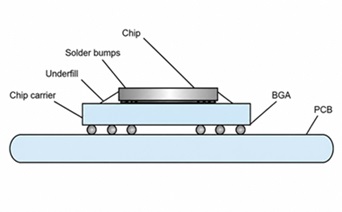
Flip chip technology traces back to IBM's work in the 1960s. Rather than wiring the chip's pads to the substrate with gold wire, the process fabricates solder or copper bumps directly on the chip's I/O pads, aligns the chip face-down onto the substrate, and reflows the bumps to form a direct metallurgical connection — hence the name "flip chip," since the die is mounted with its active circuitry facing the substrate instead of facing up. Underfill epoxy is then dispensed into the resulting gap to lock in electrical, thermal, and mechanical reliability.
Industrial adoption accelerated through the 1990s, largely driven by Ball Grid Array (BGA) packaging. As I/O counts on individual dies climbed toward and past 1,000 pads, wire bonding could no longer keep up with density or performance requirements — which is what pushed the industry toward flip chip interconnects and gave rise to FC-BGA, now a mainstream format across high-performance computing and mobile chips alike.
The Flip Chip Process Flow
Bump fabrication is the first stage of any flip chip assembly process, and the method chosen shapes everything downstream. Three approaches dominate: thermosonic bonding (gold bumps, suited to lower I/O density), solder reflow (moderate density, 40–50μm pitch), and thermocompression bonding, or TCB (fine-pitch copper pillar bumps down to 10–40μm pitch, enabling the highest interconnect density available today). Copper pillar bumps have become the preferred choice for most advanced designs, offering strong electrical and thermal performance at a lower cost than gold. Under-bump metallization (UBM) — deposited via sputtering, electroless plating, or electroplating — sits between the aluminum bond pad and the bump itself, improving adhesion and conductivity.
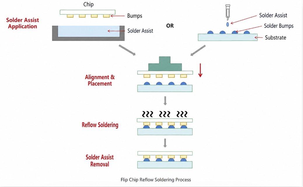
Alignment and bonding come next. High-precision placement equipment aligns chip bumps to substrate pads with submicron accuracy. Flux is applied to remove oxides and promote wetting, the die is placed automatically, and the assembly is run through a tightly controlled reflow profile to form the joint before flux residue is cleaned away. For very high bump counts and the finest pitches, standard reflow can run into thermal warpage and alignment error — which is exactly where thermocompression bonding flip chip processes take over, applying heat and pressure directly for a more controlled result.
Underfill closes out the process. The narrow gap beneath the bump array — known as the C4 zone (Controlled Collapse Chip Connection) — is filled with epoxy to prevent joint shifting, cold joints, or bridging under thermal and mechanical stress. The two dominant approaches are capillary underfill (CUF), where epoxy is dispensed along the die edge and drawn through the gap by capillary action before curing, and molded underfill (MUF), which combines encapsulation and underfill into a single transfer-molding step for higher throughput.
Advantages and Limitations
The case for flip chip assembly comes down to four things: high packaging density with shorter signal paths and a smaller footprint; superior electrical performance from lower parasitic resistance, inductance, and capacitance; excellent thermal conductivity, since heat dissipates through the substrate rather than through bond wires; and simplified assembly overall, since eliminating the wire bonding step reduces both process complexity and cost.
That said, flip chip isn't without trade-offs. Wafer-level bumping requires specialized infrastructure and adds process steps. Dies not originally designed for flip chip often need a redistribution layer (RDL) to reroute I/O. And CTE (coefficient of thermal expansion) mismatch between silicon and substrate materials makes flip chip assemblies particularly sensitive to thermal stress, demanding careful material selection and thermal analysis.
Outlook
Flip chip has come a long way — from early demonstrators with a handful of bumps to devices carrying over 100,000 I/Os at pitches as fine as 20μm. It now faces real competition from Fan-Out Wafer-Level Packaging (FOWLP) and Package-on-Package (PoP), both of which have found strong footholds in flagship smartphones and increasingly in high-performance SoCs above 120mm². Even so, continued innovation in materials, bump technology, and equipment keeps pushing flip chip assembly toward higher density and better performance, and it remains a cornerstone technology for next-generation electronic systems across the semiconductor industry.