A Trustworthy PCB and Electronic Manufacturing Enterprise! Contact Us



A high-performance photoresist PCB board serves as the foundational backbone of modern electronic manufacturing, enabling the precise, microscopic circuit patterning that powers consumer electronics, AI servers, and advanced semiconductor packaging. While most industry discussions focus heavily on photoresist applications in wafer chip fabrication, its equally critical role in printed circuit board production is often overlooked by beginners and even seasoned electronics enthusiasts. For every high-density, high-reliability PCB that ends up in commercial devices, industrial equipment, or high-end computing hardware, photoresist material defines the overall circuit accuracy, production yield, and long-term operational stability.
Over nearly a century of continuous technical iteration, photoresist has evolved from a simple photosensitive etching material into a diversified, industry-specific chemical solution. It no longer only supports ultra-fine lithography for semiconductor chips but has become an indispensable process material widely adopted in display panel manufacturing and mainstream PCB mass production. In the sophisticated manufacturing workflow of modern printed circuit boards, the coordination between photoresist formulas and PCB board processing techniques directly determines whether manufacturers can produce high-precision, high-density, and high-reliability circuit boards that meet the demands of next-generation electronic products.
What Is Photoresist and How Does It Work?
Photoresist, also known as photo-resist or photosensitive resist, is a specialized thin-film polymer material whose chemical solubility changes predictably under exposure to ultraviolet light, electron beams, ion beams, or X-rays. This unique photosensitive characteristic allows manufacturers to transfer pre-designed circuit patterns onto substrate surfaces accurately and form corrosion-resistant protective layers during etching and development processes.
Unlike general industrial coatings or adhesives, industrial-grade photoresist is a highly formulated composite material composed of four core components: photoinitiators, photosensitive resin, solvent carriers, and functional additives. Each component plays an irreplaceable role in adjusting the material’s sensitivity, resolution, flexibility, and etching resistance, collectively shaping the performance of the final photoresist PCB board product.
The photoinitiator is the most critical functional component of photoresist. As the core photosensitive agent, it absorbs specific wavelengths of light energy in the ultraviolet and visible light bands, triggering photochemical reactions that generate free radicals or cations. These active substances further initiate monomer polymerization and cross-linking curing, forming a stable solid film structure. The quality and formula of photoinitiators directly control the photoresist’s photosensitive speed and pattern resolution, which is why high-end PCB photoresist relies heavily on advanced fine chemical synthesis technology.
Photosensitive resin acts as the main structural carrier of photoresist, supporting the overall material framework and bonding all chemical components into a unified system. It provides essential physical and chemical properties for the cured film, including etching resistance, surface hardness, substrate adhesion, and mechanical flexibility. In industrial production, free radical polymerization is the most mature and widely applied resin synthesis process, while living radical polymerization technology remains in the laboratory iteration stage and has not yet achieved large-scale industrial mass production. The upgrading of resin technology is the fundamental driving force for improving the precision level of photoresist PCB board manufacturing.
Solvents occupy the largest proportion in the photoresist formula, mainly functioning to dilute solid raw materials and maintain the photoresist in a uniform liquid state for convenient coating, spraying, and lamination operations. It is worth noting that high-purity solvents only adjust the physical state of the material and hardly affect the core chemical properties and photosensitive performance of photoresist, ensuring the stability and consistency of batch production.
Functional additives are exclusive proprietary compounds developed by electronic chemical enterprises. They do not change the basic attributes of photoresist but can precisely adjust specific characteristics such as surface flatness, defoaming performance, storage stability, and environmental adaptability according to different PCB production scenarios, making photoresist products more adaptable to diverse and complex processing requirements.
The Essential Role of Photoresist in Modern PCB Manufacturing
Printed Circuit Boards (PCBs) are the most fundamental substrate materials in the global electronics industry. All electronic devices, from consumer smartphones, tablets, and wearable devices to industrial control equipment, automotive electronics, and high-performance AI servers, rely on PCBs to realize electronic component installation, circuit connection, and signal transmission. In the entire PCB manufacturing cost system, photoresist materials only account for about 3% of the total production cost, yet they dominate the upper limit of circuit precision, product yield, and long-term operational reliability.
In the field of high-end PCB manufacturing, especially for AI server motherboards, high-density interconnect (HDI) boards, and IC packaging substrates, the technical requirements for photoresist are extremely stringent. These advanced boards require ultra-fine circuit lines, tiny hole spacing, and stable layer-to-layer alignment, which cannot be achieved without high-precision photoresist lithography technology. The application iteration of photoresist directly promotes the upgrading of PCB products from single-sided and double-sided boards to multi-layer boards, flexible boards, and ultra-high-density precision boards.
Currently, photoresist used in PCB mass production is mainly divided into three categories: dry film photoresist, wet film photoresist, and solder resist ink. Among them, dry film and wet film photoresist are core materials for circuit pattern forming, while solder resist ink is used for final board surface protection and insulation packaging. The biggest difference between dry film and wet film lies in the coating and attaching process, and each has unique application advantages and scenario adaptability.
Wet film photoresist is directly coated on the surface of the PCB substrate in a liquid state. It features high pattern resolution, low comprehensive cost, and fast development and etching speeds, showing excellent cost performance in conventional precision PCB batch production. It is the preferred material for many medium and low-end circuit board manufacturers to balance precision and production efficiency.
Dry film photoresist is produced by pre-coating formulated liquid photoresist on a carrier thin film and processing it into a stable solid photosensitive film. During PCB production, the dry film is directly laminated on the copper-clad substrate under specific heating and pressure conditions. The greatest advantage of dry film is its excellent adaptability in special processes such as hole flooding processing. Unlike wet film, which easily penetrates into substrate holes and causes residual dirt and subsequent cleaning difficulties, dry film can perfectly avoid hole blockage problems, ensuring the smooth progress of subsequent drilling, electroplating, and shaping processes. Therefore, dry film photoresist has become the most widely used photosensitive material in high-end PCB manufacturing.
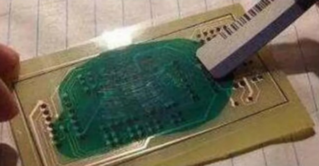
The complete working principle of dry film photoresist in PCB production is mature and standardized. First, the solid dry film is tightly laminated on the surface of the copper-clad board through thermal compression bonding. Then, precise exposure and development processes are adopted to completely copy the circuit pattern on the mask plate to the dry film surface. Finally, relying on the excellent etching resistance of the cured photoresist film, the exposed copper foil area is accurately etched, and the designed fine copper circuit is retained, completing the core pattern forming process of the photoresist PCB board.
Current Situation and Upgrading Trend of PCB Photoresist Industry
Driven by the rapid development of artificial intelligence, cloud computing, big data, and new energy electronics, the global PCB industry is undergoing a comprehensive structural upgrade. Traditional low-precision single and double-sided boards are gradually being replaced by high-value-added multi-layer boards, flexible PCBs, HDI boards, and advanced packaging substrates. Electronic terminal products are increasingly pursuing miniaturization, high integration, and high signal transmission efficiency, which puts forward higher and stricter requirements on the precision, stability, and environmental adaptability of supporting photoresist materials.
To adapt to the high-precision development trend of the PCB industry, the supporting electronic chemical industry represented by photoresist is also continuously carrying out technological innovation and formula iteration. The entire industrial chain of PCB photoresist presents a layered and collaborative development pattern, covering five core links that restrict product performance and industrial upgrading.
First, the terminal photoresist product link for PCBs. As the direct application material for circuit pattern forming, high-quality PCB photoresist is the core guarantee for improving circuit precision. It is a rigid demand material for high-end products such as AI computing boards, HDI high-density boards, and FC-BGA packaging substrates, and directly determines the market competitiveness of downstream PCB manufacturers.
Second, the core raw material link of photoresist. Electronic special resin and high-purity photoinitiator are the key raw materials that determine the upper limit of photoresist performance. For a long time, the synthesis technology of high-end raw materials has been monopolized by international leading enterprises, which has become the core bottleneck restricting the domestic substitution of high-end photoresist and the upgrading of the photoresist PCB board manufacturing industry.
Third, the supporting electronic chemical link. Photoresist lithography production cannot be completed independently. Supporting materials such as professional developer, etching solution, and cleaning agent directly affect the production yield and processing efficiency of PCBs. The collaborative upgrading of the entire chemical system is an important foundation for large-scale high-precision PCB production.
Fourth, functional film and coating materials. Special protective films and board surface coating materials can effectively isolate moisture, oxidation, and electromagnetic interference in the external environment, protect fine circuits from damage, and greatly extend the long-term stable operation life of PCB products, which is an indispensable auxiliary guarantee for high-end circuit boards.
Fifth, advanced packaging photolithography materials. With the rapid rise of high-bandwidth memory (HBM) and advanced chip packaging technology, higher requirements have been put forward for the precision and stability of packaging substrate photoresist. This link has become the core growth track of the PCB photoresist industry in the long term, leading the continuous technological progress of the entire industry.
Why High-Quality Photoresist Determines PCB Product Competitiveness
In the increasingly competitive global electronic manufacturing market, the precision difference of PCB products is essentially the difference in supporting electronic chemical materials. Many PCB manufacturers face problems such as low product yield, unstable circuit precision, and poor product consistency, most of which stem from the performance defects of low-end photoresist materials.
High-quality photoresist has ultra-high photosensitive uniformity and pattern reduction accuracy, which can meet the processing requirements of ultra-fine lines and tiny spacing of high-end PCBs. It has strong adhesion to copper foil substrates and will not fall off or shift during high-temperature etching and electroplating processes, effectively avoiding circuit short circuits, open circuits, and pattern distortion. At the same time, excellent etching resistance ensures that the designed circuit pattern can be completely and accurately presented, greatly improving the finished product qualification rate and reducing the production cost of defective products.
In addition, high-performance photoresist has good environmental adaptability, with stable physical and chemical properties in high-temperature, high-humidity, and complex electromagnetic environments. It can ensure that the PCB circuit will not deform or fail during long-term operation, improving the service life and reliability of electronic terminal products. For AI servers, automotive electronics, and industrial control equipment that require long-term stable operation, the value of high-quality photoresist is particularly prominent.
Future Development Prospects of PCB Photoresist
With the continuous deepening of global electronic manufacturing upgrading and domestic substitution of electronic chemicals, the PCB photoresist market is ushering in a sustained growth cycle. The iteration of downstream terminal products continues to drive the technological upgrading of photoresist materials, and high-precision, high-stability, and environmentally friendly low-carbon photoresist products will become the mainstream of the market.
In the field of high-end packaging and high-density circuit boards, the demand for ultra-fine lithography photoresist is growing rapidly. The research and development of new resins, efficient photoinitiators, and environmentally friendly solvent formulas will become the core direction of enterprise technological breakthroughs. At the same time, with the improvement of global environmental protection standards, low-VOC, non-toxic, and recyclable green photoresist will gradually replace traditional high-pollution products, promoting the green and sustainable development of the entire photoresist PCB board manufacturing industry.
In conclusion, photoresist is not only a core material for semiconductor chip manufacturing but also an indispensable basic material for the iterative upgrading of the global PCB industry. From ordinary consumer electronic circuit boards to high-end server computing boards and advanced packaging substrates, photoresist silently supports the precision manufacturing of all electronic equipment. In the future, with the continuous breakthrough of domestic electronic chemical technology, high-performance PCB photoresist will further realize independent controllability, empower the high-quality development of the global electronic manufacturing industry, and become an important driving force for the innovation and upgrading of the precision circuit manufacturing field.