A Trustworthy PCB and Electronic Manufacturing Enterprise! Contact Us



Learning how to use universal pcb is a practical way to build and test electronic circuits before designing a custom PCB. A universal PCB, also known as a prototyping board or perfboard, provides a regular grid of copper pads where electronic components can be mounted and connected manually.
What Is a Universal PCB?
For beginners, how to use universal pcb is an important first step in learning basic circuit prototyping. A universal PCB allows components to be arranged and connected manually, making it useful for testing circuit ideas before moving to a custom PCB.
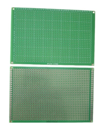
Unlike a finished PCB, a universal PCB does not have predefined copper traces connecting the components. Instead, the required electrical connections are created using component leads, solder, or connecting wires.
Understanding the structure of the board is important before starting. On a typical universal PCB, individual copper pads are not automatically connected to each other. This is different from a breadboard, where specific groups of holes are internally connected.
What Do You Need?
Before starting, prepare a universal PCB, electronic components, a soldering iron, solder wire, tweezers, wire cutters, connecting wires, and a multimeter.
A temperature-controlled soldering iron can be useful for beginners because the temperature can be adjusted according to the size of the solder joint. You should also have the circuit schematic available throughout the assembly process.
How to Use a Universal PCB Step by Step
1. Plan the Circuit Layout
Start with the circuit schematic and identify the main components, power connections, ground connections, and signal paths.
Before soldering anything, decide where each component should be placed. Components that need to connect to each other should generally be positioned close together.
A well-planned layout makes the circuit easier to assemble and troubleshoot. It also reduces the amount of wiring required on the back of the board.
2. Insert the Components
Insert resistors, capacitors, LEDs, IC sockets, connectors, and other through-hole components into the appropriate holes.
Pay particular attention to component orientation. LEDs, diodes, electrolytic capacitors, and many integrated circuits have polarity or a specific orientation that must be followed.
Once the main components are positioned, compare the physical layout with the schematic before soldering.
3. Secure the Components
After inserting a component, slightly bend its leads on the back of the board to keep it in position.
For larger components such as connectors, switches, or transformers, make sure they are firmly positioned before soldering.
Avoid cutting the leads immediately. Keeping some extra length can make it easier to correct a wiring mistake during the prototype stage.
4. Solder the Components
Place the soldering iron tip so that it contacts both the copper pad and the component lead.
Apply a small amount of solder to the heated joint and allow it to flow around the lead and pad. Remove the solder first, then remove the soldering iron.
A good solder joint should securely connect the component lead to the copper pad without excessive solder.
Too much solder can unintentionally connect neighboring pads and create a short circuit.
5. Wire the Circuit
Once the components are soldered, create the electrical connections according to the schematic.
This is where how to wire a universal PCB becomes particularly important. Because the copper pads on a typical universal PCB are individually isolated, connections between different pads must be created manually.
Component leads can sometimes be used to connect nearby points, while insulated wires or jumper wires are better for longer connections.
Start with the power and ground connections, then work through the remaining signal paths one at a time. Keeping the wiring short and organized will make later testing much easier.
6. Trim the Leads
After confirming that a component and its connection are correct, use wire cutters to remove the excess lead.
Avoid leaving unnecessarily long metal leads because they can touch neighboring pads and cause accidental short circuits.
7. Test the Circuit
Before applying power, inspect every solder joint and connection.
Use a multimeter to check continuity and look for possible shorts between power and ground. Check the polarity of components and verify that important connections match the original schematic.
Testing before powering the circuit can prevent a small wiring mistake from damaging an IC or another component.
Common Mistakes to Avoid
One of the most common mistakes when using a universal PCB is assuming that neighboring holes are electrically connected. On most universal PCBs, the copper pads are isolated, so the circuit must be wired manually.
Another common problem is poor component placement. If components are packed too closely together, soldering becomes more difficult and accidental shorts are more likely.
Long and disorganized wires can also make troubleshooting harder. Try to keep the wiring simple and separate power, ground, and signal connections where possible.
Component polarity should also be checked carefully. Installing an LED, diode, or electrolytic capacitor in the wrong direction can prevent the circuit from working or potentially damage the component.
Universal PCB for Prototyping
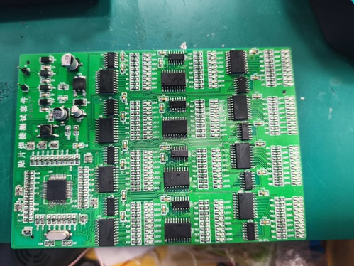
A universal PCB is particularly useful during the early development stage because it allows engineers and hobbyists to experiment with a circuit without manufacturing a dedicated board.
It is a practical choice for simple circuits, one-off projects, educational experiments, and early prototypes where the design may still change.
However, manual wiring becomes less practical as a circuit grows more complex. A prototype with many components and wires can become large, difficult to troubleshoot, and less consistent between builds.
When Should You Move to a Custom PCB?
A universal PCB is usually a development tool rather than the final solution.
Once the circuit has been successfully tested, a custom PCB becomes more appropriate when you need to manufacture multiple units, reduce the size of the design, improve reliability, or simplify assembly.
Custom PCB manufacturing is also important when a project requires multilayer routing, fine-pitch components, controlled impedance, high-speed signal integrity, or repeatable production quality.
High-frequency and RF circuits are another example. Their electrical performance depends heavily on PCB layout, trace geometry, dielectric properties, and impedance control, which are difficult to reproduce with manually connected wires.
In this sense, a universal PCB can serve as the practical bridge between an initial circuit idea and a manufacturable PCB design.
Final Thoughts
A universal PCB provides a simple and flexible way to test electronic circuits before committing to a finished board. By planning the layout, installing components carefully, soldering each connection correctly, and checking the circuit before applying power, beginners can build functional prototypes with relatively little equipment.
For simple experiments, a universal PCB may be enough. Once the design has been validated and requires better reliability, smaller dimensions, or repeatable production, moving to a custom PCB is the natural next step. Learning how to use universal pcb is therefore not only a useful prototyping skill but also a practical first stage in the PCB development process.