A Trustworthy PCB and Electronic Manufacturing Enterprise! Contact Us



Are you looking to understand how an hdi multilayer pcb facilitates the design of modern, compact, and high-performance electronics? In today's fast-paced electronics market, the demand for smaller devices with greater computing power has never been higher. Traditional printed circuit boards often struggle to keep up with the physical and electrical constraints of modern engineering. This is where high-density interconnect technology steps in, transforming how hardware engineers approach complex routing, signal integrity, and miniature form factors.
Whether you are designing a sleek new smartphone, an advanced wearable device, or high-end automotive electronics, mastering the nuances of advanced circuit board architecture is essential. Let us explore what makes these specialized boards indispensable, how they differ from conventional alternatives, and what you need to consider during the design phase.
What is an HDI Multilayer PCB?
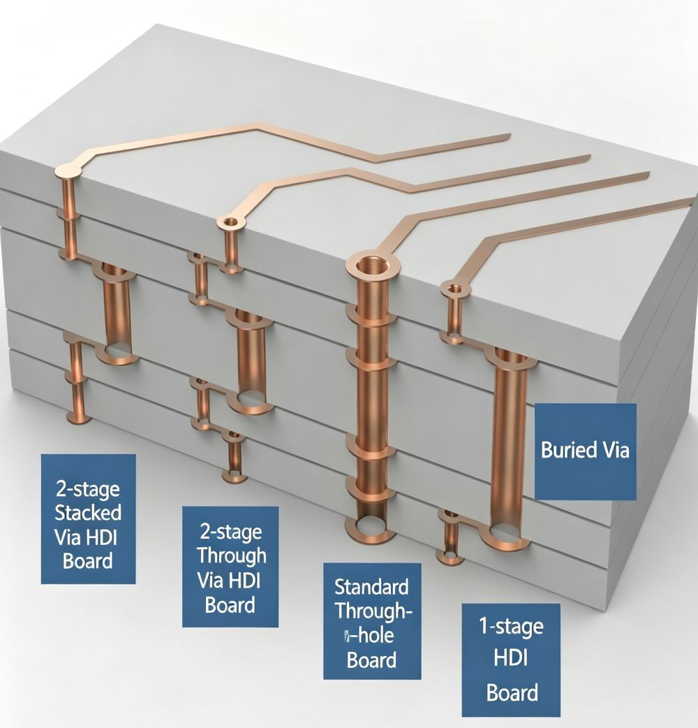
At its core, an hdi multilayer pcbrepresents a circuit board manufactured using high-density micro-fine wiring and micro-via technologies. Unlike traditional boards that rely heavily on mechanical drilling through-holes, high-density interconnect boards utilize micro blind and buried via technologies to achieve a much higher circuit distribution density.
These advanced boards consist of internal and external layers bound together through precision drilling, laser processing, and metal plating. They are typically fabricated using a build-up process. The number of build-up layers directly correlates with the technical sophistication of the board. While standard versions might feature a single build-up layer, high-end applications often employ secondary or higher-tier lamination technologies, paired with stacked vias, copper-filled plating, and direct laser drilling.
When a conventional board design exceeds eight layers and grows overly complex, switching to an hdi multilayer pcb often proves more cost-effective than traditional multi-lamination processes. Furthermore, these boards streamline advanced packaging techniques, delivering superior electrical performance, enhanced signal accuracy, and better mitigation against radio frequency interference (RFI), electromagnetic interference (EMI), electrostatic discharge (ESD), and thermal dissipation.
Why Mechanical Drilling Hits a Wall
Traditional PCB manufacturing relies heavily on mechanical drill bits. However, physics imposes severe limitations here. Once a drilled hole diameter approaches 0.15mm, production costs skyrocket, and further scaling becomes nearly impossible due to tool breakage and wear.
Modern high-density interconnect technology completely bypasses this bottleneck by utilizing advanced laser drilling methods. Laser micro-vias typically feature diameters ranging from 3 to 6 mils (0.076 to 0.152mm), paired with trace widths of 3 to 4 mils (0.076 to 0.10mm). Because pad sizes shrink dramatically, engineers can pack significantly more routing channels into a single unit area. This high-density routing environment enables the seamless placement of dense fine-pitch components such as BGAs (Ball Grid Arrays) and QFPs (Quad Flat Packages).
Key Advantages of High-Density Interconnect Boards
Engineers and product designers choose this technology for several compelling reasons:
1. Increased Routing Density: Conventional circuit boards require fan-in and fan-out routing to connect components, consuming valuable surface area. Micro-via technology allows designers to hide routing layers beneath the surface, connecting pads and traces directly via blind vias. This frees up precious outer layer estate for placing miniature components like mini-BGAs or chip-scale packages (CSPs).
2. Light, Thin, Short, and Small: By maximizing routing density per square millimeter, devices achieve their required functionality within a fraction of the physical footprint. Fewer overall layers are needed for complex logic, resulting in remarkably thin, lightweight enclosures.
3. Compatibility with Advanced Packaging: Traditional mechanical drilling cannot support the microscopic pad sizes required by modern chip packaging. Micro-via technology effortlessly accommodates cutting-edge packaging techniques like matrix packaging, CSPs, and direct chip attach (DCA) methods.
4. Superior Electrical Performance and Signal Integrity: Micro-vias are exceptionally short and narrow. This physical characteristic minimizes parasitic inductance and capacitance, drastically reducing signal reflection, crosstalk, and switching noise during high-speed data transmission.
5. Enhanced Reliability and Thermal Properties: With a low aspect ratio (often 1:1) and thinner dielectric layers, micro-vias offer higher structural reliability under thermal stress compared to standard through-holes. Additionally, the specialized dielectric materials used often feature higher glass transition temperatures, improving overall thermal management.
6. Effective EMI, RFI, and ESD Mitigation: Micro-via technology enables designers to place ground planes closer to signal layers, naturally shielding the system against electromagnetic and radio frequency interference. It also allows for a greater abundance of grounding paths, safely routing sudden electrostatic surges away from sensitive microprocessors.
7. Streamlined Design Efficiency: Shifting complex routing to internal layers opens up vast amounts of layout space, boosting overall engineering productivity and shortening time-to-market cycles.
Distinguishing Between PCB Generations
Navigating board complexity often involves understanding layer tiers.
- Single-Stage (1-HDI): Relatively straightforward to manufacture, offering a single layer of micro-vias on top or bottom cores.
- Multi-Stage (2-HDI, 3-HDI, and Beyond): Increasingly complex. Secondary or higher tiers involve intricate alignment, sequential pressing, drilling, and copper filling. Designers can choose staggered micro-vias or stacked micro-vias depending on thermal and electrical requirements. For instance, high-end consumer hardware chips frequently utilize multi-stage configurations like 5-HDI mainboards.
It is worth noting that while all standard hdi multilayer pcbsinclude blind and buried vias, simply having an embedded buried via does not automatically classify a board as high-density; the defining factor remains the integration of micro-fine blind routing and laser-drilled micro-vias.
Practical Design Considerations for Engineers
When drafting layout files for production, keep the following manufacturing guidelines in mind:
- Laser hole diameters should generally target 0.076 to 0.15mm (3 to 6 mils), maintaining an annular ring width of at least 3 mils.
- Laser holes should never be routed as raw through-holes across the entire board; internal dielectric layer thickness should remain under 0.1mm.
- The copper thickness on layers processed by laser drilling and direct connection should not exceed 1 oz.
- Stack-up designs must remain perfectly symmetrical. Total layer counts should ideally be even, keeping copper weights and core dielectric thicknesses balanced to prevent warping during high-temperature lamination.
Standard FR-4 Boards vs. High-Density Alternatives
Traditional printed circuit boards primarily utilize FR-4 material, consisting of woven glass fabric saturated with epoxy resin. Historically, traditional high-density manufacturing required specialized adhesive-backed copper foil on outer layers because early laser drilling systems struggled to cleanly pierce woven glass cloth.
Today, however, high-energy ultraviolet and laser systems can effortlessly penetrate standard glass-reinforced prepreg materials like 1180 glass cloth. This technological leap means that modern fabrication houses can build an hdi multilayer pcballongside conventional laminate stacks with minimal disruption, making high-performance circuit architecture more accessible and affordable than ever before.
As consumer electronics continue their relentless march toward miniaturization, higher efficiency, and greater processing speeds, adopting advanced high-density interconnect strategies is no longer just an optional upgrade—it is a fundamental requirement for staying competitive in modern hardware engineering.