A Trustworthy PCB and Electronic Manufacturing Enterprise! Contact Us



PCBs play a vital role in the rapidly evolving fields of automation and electronics. Over time, PCBs have evolved into various versions and types to meet specific application needs and improved standards. The Ball Grid Array (BGA) is one of the most advanced and compact PCB configurations. Size constraints often present a challenge for BGA PCB and product designers, as many applications require high-performance, compact devices. The use of BGA technology represents a significant innovation in compact PCB design.
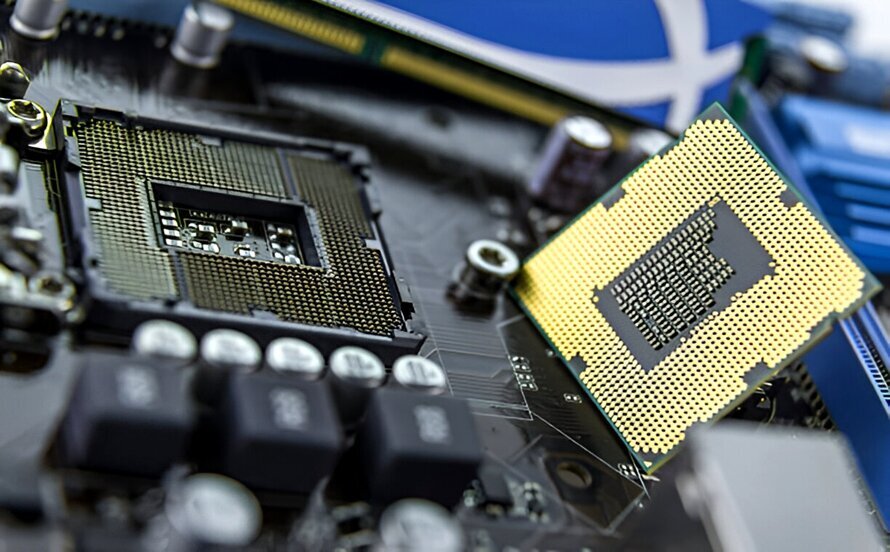
BGA PCB
What is a BGA PCB?
A BGA PCB is designed and manufactured specifically to support Ball Grid Array (BGA) components. BGA components are integrated circuits (ICs) featuring a compact ball-grid interconnect design that enables high I/O (input/output) density. The laminate materials used for BGA PCBs vary based on the heat dissipation and signal integrity requirements of the end application. Common laminate materials include FR4, high-Tg materials, and polyimide substrates.
BGA PCB Design Guidelines and Manufacturing Process
As previously noted, proper design is crucial when placing Ball Grid Arrays on a PCB. Improper design practices can lead to issues requiring rework and increase production costs. Several rules apply to BGA designs, including the following:
Array Design and Type
Ensure the array fits the board dimensions or the required footprint. The spacing between pads varies but generally ranges from 0.8 mm to 1 mm. Some designs utilize solder mask-defined pads, while others do not.
Various BGA types are available. Select the array that best suits your specific application. Options include plastic, ceramic, micro-BGA, ultra-fine BGA, stacked BGA, as well as leaded and lead-free variants.
BGA PCB Pad Size and Shape
Most boards featuring Ball Grid Arrays comply with IPC Class 3 standards, which mandate strict reliability levels. This entails tighter tolerances and specific requirements for solder mask and annular ring features.
Determine pad dimensions based on the size of the solder balls. Decide whether the pads should be solder mask-defined.
For optimal results, use circular pads. Compared to rectangular pads, these pads offer superior wetting characteristics, resulting in excellent solder joints and secure connections.
Successful BGA PCB manufacturing relies on rigorous process control and well-maintained equipment. The production steps for BGA PCBs are outlined below.
Inner layer fabrication: First, the copper foil surface is cleaned to remove contaminants and oxides. Photoresist is then applied to the copper layer, followed by UV exposure and chemical development. Finally, excess copper is etched away.
Lamination: Layers consisting of prepreg and core materials are stacked and bonded together using heat and pressure. Precise alignment of the layers is essential to prevent inner-layer shifting.
Drilling and via plating: Vias or holes in the BGA PCB are created using mechanical or laser drilling. This is followed by a deburring process—using plasma or chemical methods—to remove excess burrs. The via surfaces are plated with electroless copper to ensure electrical conductivity.
Outer layer patterning: Similar to the inner layer process, outer layer patterning uses photolithography to create circuit patterns on the PCB. Copper pads and traces are precisely etched to ensure reliable component mounting.
Solder mask application: A solder mask is applied over the copper to provide protection. This prevents solder bridging, leakage, and oxidation of the copper circuitry.
Silkscreen printing: Adding reference designators, fiducial marks, and traceability information to the PCB is crucial. This is achieved through silkscreen printing, a process used to print labels and markings onto the board.
Surface finish: BGA PCB pads require a surface finish to prevent copper oxidation. Processes such as ENIG (Electroless Nickel Immersion Gold) are used; these also facilitate strong bonding between BGA components and the copper surface.
What are the applications of BGA PCBs?
Due to their high reliability and compact size, BGA PCBs are highly favored across various sectors of the electronics market. Key application areas include:
Consumer electronics: The compact size of BGA PCBs makes them widely used in consumer electronic devices such as laptops, tablets, and smartphones. The use of Ball Grid Array (BGA) packaging in design shortens circuit paths, thereby reducing risks associated with inductance and resistance.
Automotive Electronics: BGA PCBs are also suitable for automotive-grade electronics. High reliability is a primary consideration for automotive equipment, such as ECUs and infotainment systems. Solder balls provide efficient heat dissipation and robust mechanical connections.
Medical Equipment: Medical devices—including wearables, imaging systems, and diagnostic equipment—require secure electronic components. High-performance BGA PCBs play a vital role in healthcare technology, enabling portability and high-speed processing capabilities.
Industrial Electronics: Automation and robotics in the industrial electronics sector require durable BGA-packaged PCBs for real-time control and monitoring. Equipment and machinery utilizing PLCs and embedded systems also employ BGA boards to achieve rapid processing, high-capacity storage, and excellent thermal performance.
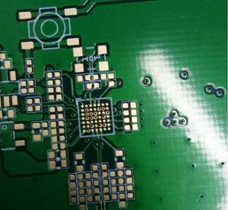
BGA PCB
As miniaturization technology continues to evolve, we are likely to see changes in BGA PCBs over the coming years. Components are becoming smaller, while IC functionality grows increasingly powerful. Furthermore, with the introduction of 5G networks and other communication technologies, BGA boards will find expanded applications due to their ability to pack more power into a smaller footprint. BGA packaging is poised to improve in the future; it will also become more reliable with the advent of newer IC technologies and high-quality materials capable of withstanding diverse operating conditions.
Successful PCB design relies heavily on BGA routing skills. This process demands careful preparation, the right techniques, and sometimes advanced software. Understanding high pin counts and signal integrity is essential for creating efficient, functional designs. Ultimately, the success of the design depends largely on the quality of your preparation.
If you are seeking assistance with a complex BGA routing project, iPCB is here to help. We possess the capabilities required to successfully execute even the most challenging designs. Please feel free to contact us to discuss your BGA PCB project and let us assist you with your BGA routing layout!