A Trustworthy PCB and Electronic Manufacturing Enterprise! Contact Us



GPS PCB design sits at the intersection of RF engineering and manufacturing precision — get it right, and a module locks onto satellites in seconds; get it wrong, and no firmware fix can save a board that can't hear the signal. This guide covers the core principles of GPS PCB design, from layout and material selection to manufacturing and quality control.
What Is a GPS PCB
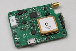
A GPS PCB is a board purpose-built to receive and process satellite positioning signals — specifically the 1575.42MHz L1-band signal — where RF performance, not general-purpose logic, drives every design decision. The signal path runs from antenna to RF front end (filtering, impedance matching, LNA, down-conversion, ADC) to a baseband chip that outputs position, velocity, and time data via NMEA-0183, alongside power regulation and UART/I2C/SPI interfaces.
Design and manufacturing quality directly determine time-to-first-fix (TTFF), positioning accuracy, receiver sensitivity, and interference immunity. GPS PCBs show up in automotive navigation, drones, wearables, asset tracking, precision timing, and surveying equipment.
Core Design Considerations
RF trace routing & impedance matching: GPS signals arrive at roughly -130dBm, so any path discontinuity causes real loss. Maintain a strict 50Ω characteristic impedance throughout the GPS antenna PCB signal path. Keep RF traces short and direct, use 45° bends instead of right angles, hold trace width/spacing tolerance to ±0.02mm, and minimize vias — adding symmetric ground vias around any RF via that's unavoidable. Reserve space for a pi- or LC-matching network near the antenna to compensate for tolerance and tune for minimum return loss.
Ground plane integrity: RF traces need a continuous, unbroken ground plane directly beneath them to form a stable microstrip/stripline structure. Separate RF, digital, and power grounds, connecting them at a single point only — never mix them across large areas. Never route slots or traces through the ground plane under RF circuitry.
EMI and interference immunity: Zone the board — antenna, RF, then digital/power — with ground copper and stitching vias forming an isolation wall between regions. Shield noisy blocks (switching supplies, high-speed digital) with metal cans, and surround the RF chip with a dense via ring to form a Faraday-cage-like structure. Give the RF chip its own supply rail with LC/RC filtering and both bulk and high-frequency decoupling capacitors, and keep crystal oscillators shielded and away from the RF section.
Antenna placement: Place the antenna at the board edge with a clear keep-out zone beneath it — no copper, vias, or metal components nearby. For external antennas, use a well-matched connector and keep the 50Ω trace as short as possible. Multi-constellation designs (BeiDou, GLONASS, Galileo) need antenna coverage and matching circuitry for each band used.
Materials and Stack-Up
FR-4 (Dk ~4.2–4.6, Df ~0.02 at 1GHz) is the standard choice for cost-sensitive consumer products. High-frequency laminates like Rogers RO4350B (Dk 3.48, Df 0.0037 at 10GHz) suit industrial and automotive-grade designs needing lower loss. A hybrid stack-up — high-frequency laminate for the RF layer, FR-4 elsewhere — is the most common approach in volume production, balancing cost and performance.
A four-layer GPS PCB (signal / ground / power / signal) is the recommended baseline: RF on top next to a solid ground plane gives good impedance control and EMI isolation at a reasonable cost. Two-layer boards work only for basic, low-performance designs; six-to-eight-layer stacks suit high-performance or multi-constellation designs needing separate RF and digital grounds.
Key manufacturing tolerances: trace width/spacing ±0.02–0.05mm (impedance within ±2Ω), 1oz copper, ENIG surface finish (avoid HASL — its uneven surface disrupts RF parameters), Dk tolerance ±0.05 on high-frequency laminates, and no solder mask or silkscreen over the antenna or RF trace areas.
Verification and Production QC
Simulate impedance and stack-up before tape-out, targeting return loss below -15dB. Validate first-article samples with a network analyzer plus open-sky/anechoic testing for TTFF, accuracy, and sensitivity, along with temperature and vibration testing. In production, sample incoming materials for Dk, thickness, and copper weight consistency, and keep RF matching components tunable to compensate for batch-to-batch variation.
GPS PCB design is fundamentally about protecting a very weak signal in a noisy environment — through disciplined impedance control, a solid ground plane, careful EMI isolation, smart antenna placement, and the right material and manufacturing choices. Get these fundamentals right, and the result is a board with fast acquisition, high accuracy, and strong interference immunity.