A Trustworthy PCB and Electronic Manufacturing Enterprise! Contact Us



1. Definition & Abstraction Layer
Circuit Diagram (Schematic)
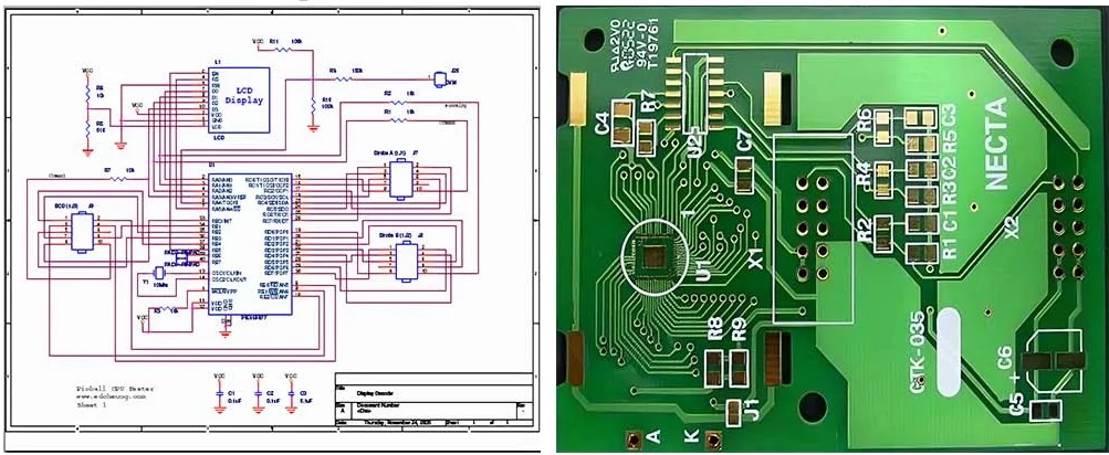
A schematic resides at the electrical abstraction layer. It uses standard IEEE component symbols and defines electrical connectivity between component pins via named electrical nets.
No geometric or physical dimension data exists inside a schematic. Its primary deliverable is the netlist, which maps every component pin to its corresponding electrical net. The netlist acts as the formal interface passed into the PCB layout tool.
Schematic answers: electrical topology, signal paths, power architecture, component selection and BOM definition.
PCB Layout
PCB Layout belongs to the physical implementation layer. Constrained by the imported netlist, designers place components within a defined board outline and stackup, design pads, route copper traces, implement blind/buried/micro vias, and define solder mask, silkscreen and assembly markers.
Layout exports Gerber, NC drill files, IPC-2581 and stackup documentation containing full geometric, layer and manufacturing parameters. This dataset is the official input for PCB fabrication.
Layout answers: geometric constraints, impedance control, signal integrity, power integrity, thermal spreading, EMC/EMI and DFM manufacturability.
Engineering takeaway:
✅ Circuit Diagram: defines electrical constraints the circuit must satisfy
✅ PCB Layout: physically implements those electrical constraints while satisfying process, thermal, EMC and reliability limits.
2. Comparison Table
Item Circuit Diagram (Schematic) PCB Layout
Abstraction Layer Electrical logic, geometry-agnostic Physical geometry (electrical + geometry + process coupled)
Core Data Netlist, BOM Gerber, NC Drill, IPC-2581, stackup, 3D CAD
Key Constraints KCL, KVL, component ratings, Trace width/spacing, impedance, dielectric thickness, hole size,
functional topology copper weight, creepage, thermal resistance, return path
Simulation Domain Circuit simulation: SPICE, DC, AC, SI signal integrity, PI power integrity, thermal simulation, EMC, stress simulation
transient analysis
Impact of Modification Alters netlist topology; changes circuit Modifies geometry only if netlist remains unchanged; function stays same, but changes circuit
function and electrical boundaries SI/PI/thermal/EMI performance varies greatly
Manufacturing Ready No, missing geometry, stackup Standard fabrication input
and process parameters
3. Design Flow: ERC → Netlist Import → DRC
Standard hardware workflow:
Complete schematic capture and run ERC (Electrical Rule Check) to catch floating pins, shorted power nets, duplicate nets and unconnected inputs. ERC validates only electrical logic, it cannot catch physical routing issues.
Export netlist and import into PCB layout software. The netlist locks pin-to-net mapping and acts as a hard constraint; routing in PCB layout must preserve netlist connectivity.
Place & route PCB layout, configure stackup and impedance rules, run DRC (Design Rule Check) to flag insufficient trace width, spacing violations, too small drill holes, pad violations and solder mask bridge issues.
Critical note: ERC ≠ DRC. ERC checks electrical rules only. DRC checks geometry and manufacturing rules only. Passing ERC does not guarantee passing DRC, and clean DRC results do not guarantee functional hardware.
4. Advanced Engineering Pitfalls
Misconception 1: Identical netlist guarantees identical board performance
False. With the same netlist, different layouts create drastically different return paths and parasitic L/C. For high-speed or high-current designs, parasitics dominate SI/PI, noise and temperature rise. Parasitics are not modelled in the schematic.
Misconception 2: Voltage/current values annotated on schematic equal real hardware behavior
False. Schematic uses idealized models. Layout introduces trace resistance, parasitic LC and ground plane splitting, which create IR drop and ground bounce. Measured values on hardware often deviate from schematic calculations.
Misconception 3: Editing PCB routing will automatically synchronize schematic
False. Schematic and PCB maintain separate databases. Any pin connectivity change must be edited on the schematic side, re-export netlist and update PCB, otherwise netlist mismatch occurs, a severe design defect.
Misconception 4: Schematic can be used for DFM review
False. DFM evaluation relies on geometry data, which is only available in Layout/Gerber. Schematic cannot verify minimum trace width, hole copper, solder mask or board clearance risks.
5. When to modify schematic vs optimize layout
Change topology, add/remove components, modify pin connections, update BOM part numbers or restructure power rails → Edit schematic, run ERC, update netlist
Reposition components, re-route traces, adjust copper weight/trace width, modify stackup, relocate decoupling capacitors or rework grounding/thermal layout → Layout-only optimization, netlist unchanged
Side note: Adding new components such as decoupling caps requires schematic edits plus BOM and netlist update.
6. Boundary of Co-Simulation
Schematic-domain SPICE simulation: validates DC operating point, transient response and loop stability, using simplified/ideal component models, ignoring PCB parasitic effects.
Layout-domain SI/PI extraction: extracts RLCG parasitics from PCB geometry to analyze transmission line effects, impedance discontinuity, plane noise and IR Drop. Depends fully on PCB layout geometry.
Recommended engineering practice: Schematic SPICE to prove functional feasibility; Layout SI/PI to quantify signal and power degradation introduced by physical implementation.
Conclusion
The circuit diagram is an abstract definition of circuit topology and electrical constraints, validated via ERC. PCB Layout is the physical realization of the circuit on substrate, validated via DRC. The netlist binds these two domains together.
A schematic determines whether a circuit can work in theory. PCB Layout determines whether it can operate stably, reliably and compliantly in physical hardware. Many hardware failures are not caused by schematic errors, but by layout-induced parasitics, poor return paths, inadequate thermal design or EMC defects.