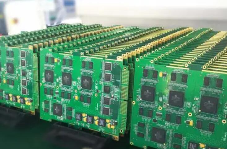
In the manufacture of PCBA, often encounter some PCBA defective products, as a PCBA foundry, iPCB according to experience, summed up some PCBA foundry in the common problems and solutions:
Solder beads
a.During the printing process, solder paste flows out of the pad due to misalignment between the template and the pad:
1.Follow up the pad,component pins and solder paste for oxidation;
2.Adjust the opening of the template to align with the pad accurately;
In the component mounting process,solder paste is placed between the chip component pins and the pad. If the pad and component pins are not well moistened (poor solderability),the liquid solder will shrink and make the solder joint insufficient,and all the solder particles will not be able to polymerise into a single solder joint. Part of the liquid solder will flow out from the solder joints and form solder beads.
b.The pressure of Z-axis during the paste process is too high to squeeze the solder paste out of the pad instantaneously:
1.Adjust the Z-axis pressure precisely;
c.Heating speed is too fast,time is too short solder paste internal moisture and solvent can not be completely evaporated,to reach the reflow soldering area caused by the solvent,moisture boiling,spattering out of the beads:
1.Adjust the preheating area activation area temperature rise rate.
d.Template opening size and profile is not clear:
1.Check whether the template opening and contour are clear,and replace the template if necessary.

PCBA
Tombstone (Manhattan Phenomenon)
Tombstone is caused by the imbalance of surface tension of solder paste on the pads at both ends of the CHIP components during the reflow soldering process,which is manifested by the components partially or completely standing up, commonly known as Tomb Stone Effect or Draw-bridging Effect, Manhattan Effect,refers to the phenomenon of buildings standing up in the Manhattan area of New York,and Manhattan Effect. Manhattan Effect,which refers to the phenomenon of buildings in New York City.Manhattan is particularly suitable for high-rise buildings due to its geology. There are more than 5,500 high-rise buildings in Manhattan,35 of which are over 200 metres tall,making it the largest concentration of skyscrapers in the world.It is the largest concentration of skyscrapers in the world, with buildings such as New York's iconic Empire State Building,Rockefeller Center,Chrysler Building,and the MetLife Tower). The smaller the component size, the more likely it is to occur.Especially in the production of 1005 or smaller 0603 SMD components,it is very difficult to eliminate the monument phenomenon.
Tombstone phenomenon and drawbridge phenomenon is relatively intuitive,easy to understand,and Manhattan phenomenon which looks a little obscure,early PCBA literature translators may be Manhattan phenomenon because the word looks more dazzling, so use more, so that now many people do not know why.
Some of the major factors are briefly analysed below:
a. Preheat period
When the preheating temperature is set lower and the preheating time is set shorter, the probability of melting solder paste at both ends of the component at different times is greatly increased,which leads to an imbalance in tension between the two ends to form a ‘monument’,which should be set correctly in the preheating period process parameters. According to the experience of Berrian, the preheating temperature is generally 150 + 10 ℃, the time is about 60-90 seconds.
b.Pad size
When designing pads for chip resistors and capacitors,the overall symmetry should be strictly maintained, i.e., the shape and dimensions of the pad pattern should be identical to ensure that when the solder paste is melted, the combined force acting on the solder joints on the components is zero,thus facilitating the formation of ideal solder joints. Design is the first step in the manufacturing process, and poorly designed pads can be a major cause of component erection. Specific pad design standards can be found in IPC-782, ‘Surface Mount Design and Pad Layout Standards’ In fact, pads that are too far over the component may allow the component to slide around while the solder is wetting, causing the component to pull out of the end of the pad.
For small chip components, designing a different pad size for one end of the component or connecting one end of the pad to the ground board may also cause the component to stand up. The use of different pad sizes may result in unbalanced pad heating and paste flow times. During reflow, the component simply floats on the liquid solder and reaches its final position as the solder cures. The varying wetting forces on the pad can cause a lack of adhesion and component rotation. In some cases, extending the time above the liquefaction temperature can reduce component erection.
c.Solder Paste Thickness
When the thickness of the solder paste is reduced, the erection phenomenon is significantly reduced. This is due to:
1.Thinner solder paste reduces the surface tension when the paste melts.
2.As the paste becomes thinner, the heat capacity of the entire pad decreases,and the probability of the paste melting on both pads at the same time is greatly increased. Solder paste thickness is determined by the thickness of the template, Table 2 is the use of 0.1mm and 0.2mm thick template monument phenomenon compared to the use of 1608 components.In general,when using 1608 components, it is recommended to use 0.15mm templates.
Common PCBA problem formation and solutions Common PCBA problem formation and solutions
d.Mounting offset
In general, the component offset generated during the paste, in the reflow process will be due to the melting of the solder paste surface tension pulling the component and automatically correct, we call it ‘self-adjustment’, but the offset is serious, pulling instead of making the component to stand up to produce a ‘monument’ phenomenon.This is because This is because
1.The solder end that has more contact with the component gets more heat capacity and melts first.
2.The two ends of the component and the adhesion of the solder paste are different.Therefore,the precision of the component should be adjusted to avoid large deviations.
e.Component weight
Lighter components ‘monument’ phenomenon of higher incidence, because the uneven tension can easily pull the components. So in the selection of components, if possible, should give preference to the size and weight of the components.
There are many welding defects, this article lists only two of the most common defects.Measures to solve these welding defects are also many, but often mutual constraints. Such as increasing the preheating temperature can effectively eliminate the monument, but there may be a large number of solder balls due to faster heating speed.This in the solution of these problems should be considered from a number of aspects, choose a compromise,this point in the actual work we should remember.

PCBA OEM
iPCB focuses on PCB design and production, component sourcing, PCBA OEM, assembly and testing, and is a one-stop PCBA electronic manufacturing service dedicated to providing customers with samples in small and medium batches.