A Trustworthy PCB and Electronic Manufacturing Enterprise! Contact Us



Against the backdrop of AI computing chips, Chiplet heterogeneous integration, 5G/6G millimeter-wave RF and Co-packaged Optics (CPO), traditional substrates including FR-4, BT resin and ABF organic carrier boards are hitting performance limits. Special glass substrates, long adopted in display panels, are rapidly expanding into PCB and microelectronic interconnection fields. They emerge as a balanced solution delivering high-frequency performance, dimensional stability and high-density wiring. This article breaks down the value, manufacturing processes, application challenges and market outlook of glass substrates for PCB and advanced packaging scenarios.
1.What Are Electronic-Grade Glass Substrates?
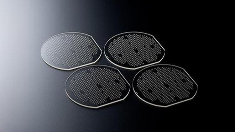
Glass substrates for electronics are typically made of borosilicate or aluminosilicate ultra-thin glass (representative brands: Schott AF32, Corning Lotus XT), with thickness ranging from 50μm to 500μm.
Different from ordinary architectural glass, they feature ultra-high surface flatness and ultra-low impurity content. Via processes such as TGV (Through-Glass Via), surface coating and RDL redistribution layers, conductive circuits can be formed on and inside glass to realize electrical interconnection.
Two easily confused concepts are clarified here:
Glass Core Substrate: A solid glass sheet acts as the core, laminated with dielectric layers and copper circuits on both sides, a modified PCB structure.
TGV Glass Interposer: Vertical vias are fabricated by laser or etching, filled with metal for interlayer connection. Widely used in 2.5D/3D advanced packaging as an alternative to silicon interposers.
2. Core Advantages Over Conventional Organic Substrates
2.1 Well-Matched CTE with Silicon Die
Traditional organic substrates have a CTE of 12~22 ppm/°C, while silicon chips only reach ~2.6 ppm/°C. Huge thermal mismatch during temperature cycling causes bump cracking, substrate warpage and pattern alignment shift.
Glass substrates feature controllable CTE at 3~5 ppm/°C, drastically reducing thermal mismatch with silicon wafers. For large-size AI chips integrated with HBM, glass can cut package warpage by more than 50% and significantly improve long-term reliability.
2.2 Outstanding High-Frequency Electrical Performance
Glass is a low-loss insulating material with Df < 0.002 at 10GHz, far superior to FR-4 and standard BT resin.
For 112Gbps / 224Gbps high-speed SerDes signals and millimeter-wave RF circuits, glass effectively reduces insertion loss, crosstalk and phase deviation. It becomes an ideal substrate for 6G communication and automotive 77GHz radar high-frequency PCBs.
2.3 Ultra-Smooth Surface Enables Ultra-Fine Wiring
The surface roughness Ra of glass substrates can be lower than 0.5nm. Combined with SAP semi-additive processes, line width/spacing of 1~3μm can be realized, exceeding the limit of conventional PCB technology, and meeting high-density interconnection requirements for AI chips with thousands of I/Os.
2.4 Superior Material Stability for Opto-Electronic Integration
Glass is non-hygroscopic, high-temperature resistant and naturally transparent. Apart from electrical routing, it can embed optical channels, making it inherently suitable for CPO co-packaging to integrate electrical and optical circuits on one panel — a capability organic PCBs cannot achieve.
3. Main Commercial Application Scenarios (Focus for PCB Industry)
3.1 HPC & AI Advanced Packaging Interposers
For GPUs, AI accelerators and Chiplet systems paired with HBM, glass substrates solve packaging warpage and high-speed signal attenuation issues, acting as an alternative to ABF organic carrier boards and silicon interposers. Intel, TSMC and Samsung have launched sample verification for glass substrate projects.
3.2 High-Frequency RF PCBs: 5G/6G & Automotive Millimeter-Wave Radar
RF circuits are extremely sensitive to dielectric loss. Glass substrates minimize signal attenuation and simplify the design of RF front-end modules, ideal for automotive radar and millimeter-wave base station circuit boards.
3.3 CPO Substrates for Opto-Electronic Co-Packaging
For optical modules and switch chip opto-electronic integration, glass substrates carry both electrical traces and optical transmission paths, becoming a core carrier for next-generation high-speed optical interconnection in data centers.
3.4 Carrier Boards for Sensors & Miniature Optical Modules
Applied in machine vision, medical imaging and compact camera modules, balancing precision dimensional stability and opto-electronic integration.
4. Bottlenecks for Mass Industrialization
Despite prominent strengths, wide adoption of glass-based PCBs still faces practical constraints, which should be communicated to clients at the early project stage:
Brittleness risk: Ultra-thin glass is prone to edge chipping and microcracks; laser cutting and drilling yield are lower than organic materials.
Interfacial adhesion challenge: Copper and glass are heterogeneous materials. Delamination risks exist under thermal cycling and humidity tests, relying on plasma activation and transition seed layer optimization.
High cost barrier: Raw material, TGV drilling and coating costs remain high for small-batch sampling. Currently glass targets high-end projects and cannot replace FR-4 fully in the short term.
Immature supply chain: Mass production lines for large-area precision coating and TGV are still under construction in China, leading to longer lead time compared with conventional PCBs.
5. Industry Outlook: Complement, Not Full Replacement
Glass substrates will not completely replace FR-4 and BT organic PCBs.
The market landscape will diverge in the medium-long run: consumer electronics, general industrial control and low-to-medium speed circuits will continue adopting mature organic substrates. Glass substrates will gain continuous penetration in high-value segments including AI packaging, high-frequency RF, CPO and heterogeneous high-density integration.
6.Conclusion
In the post-Moore era, chip performance improvement no longer relies solely on wafer scaling. Innovations in system packaging and substrate materials become critical breakthrough points. With unique combined electrical, mechanical and optical properties, specialty glass substrates open a brand-new technical window for PCB and microelectronic interconnection. As TGV processes mature and manufacturing costs decline, glass-based PCB solutions will gradually move from lab samples to mass commercialization within the next 3–5 years.