A Trustworthy PCB and Electronic Manufacturing Enterprise! Contact Us



Organic substrate technology sits at the intersection of two industries that are often discussed separately but are, in practice, deeply connected: PCB manufacturing and semiconductor packaging. As an IC substrate (also called a package substrate), the organic substrate serves as the critical interconnect layer between the silicon die and the PCB — and its performance increasingly determines how much power, speed, and density a finished electronic system can deliver.
Understanding where organic substrates fit requires drawing a clear line between two related but distinct product categories. Traditional PCB base materials — think FR-4 laminate and copper-clad boards — are one branch of the organic substrate family. The other, more advanced branch is the organic package substrate used in flip chip and BGA packaging, where line widths shrink from tens of microns down to just a few. This is also the branch where the organic substrate vs ceramic substrate comparison usually comes up, since ceramic has long been the alternative material of choice for high-reliability, high-frequency packaging.
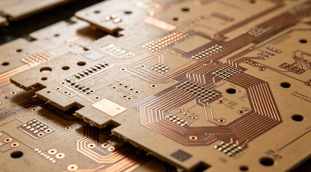
Within the package substrate category, two materials dominate the conversation: ABF substrate and BT substrate. ABF (Ajinomoto Build-up Film) has become the material of choice for high-performance computing, with organic substrate for AI chips and advanced GPUs relying heavily on ABF's fine-line capability and superior electrical performance at high frequencies. BT (Bismaleimide Triazine) substrates, by contrast, offer a more cost-effective option and remain widely used in memory packaging and general-purpose IC substrates where extreme line density isn't the primary requirement.
Why Organic Substrates Matter for Flip Chip Packaging
In flip chip substrate designs, the die is mounted face-down directly onto the substrate, with solder bumps replacing traditional wire bonds. This approach demands extremely tight registration accuracy and low signal loss — both areas where organic substrates, particularly ABF-based builds, have continued to push the envelope. As chip designs move toward chiplet architectures and heterogeneous integration, the substrate is no longer a passive carrier; it's an active contributor to system-level performance, thermal management, and signal integrity.
Sourcing Considerations: Organic Package Substrate China
Manufacturing capability for advanced organic package substrates has historically been concentrated among a small number of global suppliers, with much of the ABF substrate supply chain based in Japan, South Korea, and Taiwan. Over the past several years, however, organic package substrate China-based manufacturing has expanded significantly, offering companies a broader base of qualified organic IC substrate manufacturers to work with — an important consideration for teams evaluating supply chain resilience and lead times alongside technical capability.
How Organic Substrates Are Manufactured
The build-up process for an organic package substrate shares some DNA with standard PCB fabrication, but runs to far tighter tolerances. It typically starts with a core layer — often BT-based or, in coreless designs, omitted entirely — onto which alternating layers of dielectric film and copper are built up one at a time. For ABF substrates specifically, each build-up layer goes through lamination, laser via drilling (down to just a few microns in diameter), copper plating, and photolithographic patterning before the next layer is added. Depending on the target application, a substrate may have anywhere from four to twenty or more build-up layers, with the highest layer counts reserved for the most demanding CPU, GPU, and AI accelerator packages.
Registration accuracy is the single biggest manufacturing challenge at this scale. Because each build-up layer must align with the ones beneath it within a few microns, even minor process drift can compound across layers and compromise the entire substrate. This is one reason the pool of qualified organic IC substrate manufacturers capable of high layer-count ABF work remains relatively small compared to the broader PCB supply base — the equipment, cleanroom conditions, and process control required are simply a different tier.
Applications Across the Electronics Landscape
Organic substrates now show up in nearly every category of advanced electronics, though the specific material and design choices vary by end use:
1. High-performance computing and AI: Data center CPUs, GPUs, and AI accelerators depend on high-layer-count ABF substrates to route signal and power across dies with tens of thousands of I/O connections. As package sizes grow to accommodate multi-die and chiplet designs, substrate warpage control and fine-line capability become just as important as raw electrical performance.
2. Mobile and consumer electronics: Application processors and memory packages in smartphones and tablets typically use thinner, more cost-efficient organic substrates — often BT-based or hybrid builds — balancing performance with the tight cost targets of high-volume consumer products.
3. Automotive electronics: ADAS processors, infotainment SoCs, and power management ICs increasingly rely on organic substrates rated for extended temperature cycling and long service life, reflecting the reliability bar automotive-grade components must clear.
4. Networking and RF: 5G infrastructure and RF front-end modules benefit from organic substrates engineered for low dielectric loss, supporting stable signal transmission at the frequencies these systems operate at.
Organic Substrate vs Ceramic Substrate: Where Each One Wins
The organic substrate vs ceramic substrate decision isn't a matter of one material being universally better — it's a trade-off. Ceramic substrates offer excellent thermal conductivity, dimensional stability, and hermeticity, which is why they still show up in some RF, power, and mission-critical aerospace applications. But they're more brittle, harder to process at fine line widths, and generally more expensive at volume. Organic substrates, by contrast, offer better cost scalability, easier integration with high-layer-count build-up processes, and design flexibility that ceramic simply can't match at the densities modern chip packages require. For most high-volume and high-performance digital applications today, that trade-off has tipped decisively in favor of organic substrates.
Where the Market Is Headed
Several forces are pushing organic substrate technology forward at once. The shift toward chiplet architectures is driving demand for substrates with more layers, finer lines and spaces, and better co-design with silicon interposers. AI infrastructure buildouts are pushing substrate sizes larger than ever before, which introduces new warpage and yield challenges that manufacturers are still working through. And sustainability pressure is starting to shape material selection too, with halogen-free resin systems gaining traction alongside the push for higher performance.
Choosing the Right Substrate Partner
For engineering teams and procurement leads evaluating substrate suppliers, the decision usually comes down to a handful of practical questions: Can the manufacturer support the line width/spacing your design requires? Is their material system (ABF vs. BT) appropriate for your frequency and thermal profile? Can they demonstrate yield and reliability data at the layer count your design calls for? And do they have a track record with the specific packaging format — flip chip, BGA, or SiP — that your product needs?
As AI accelerators, high-performance computing, and next-generation automotive electronics continue to push the limits of interconnect density, the organic substrate will remain a central, if often overlooked, piece of the puzzle — bridging silicon and system in a way that shapes everything built on top of it.