A Trustworthy PCB and Electronic Manufacturing Enterprise! Contact Us



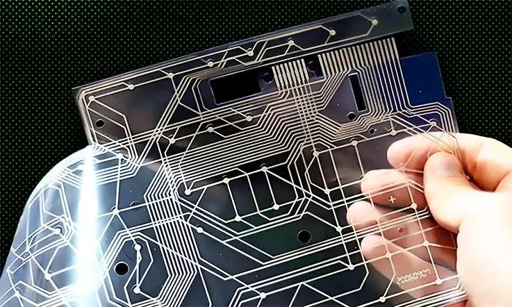
Driven by high-frequency communication, high-computing packaging and electronic miniaturization trends, glass substrates have become a critical next-generation solution for advanced PCB and IC packaging. Featuring ultra-low dielectric loss, near-zero thermal expansion, atomic-level flatness and excellent optical transparency, glass substrates effectively solve the performance bottlenecks of traditional organic substrates. This paper systematically summarizes the material characteristics, core manufacturing processes, and mainstream applications of glass-based PCBs, providing practical technical references for high-end packaging engineering.
Material Upgrade: From Organic PCB to Inorganic Glass Substrate
Traditional PCBs mainly adopt FR-4, BT resin and PTFE materials. Although mature in mass production, organic substrates show obvious limitations in millimeter-wave and high-power chip scenarios. High-frequency operation causes rising dielectric loss and deteriorated signal integrity. Large CTE mismatch between organic materials and silicon chips leads to severe thermal warpage, solder cracking and low assembly yield. In addition, high surface roughness restricts ultra-fine wiring, and hygroscopicity causes unstable electrical performance in complex environments.
Glass substrates, including borosilicate, quartz and aluminosilicate glass, have evolved from display panel materials to advanced packaging substrates after 2020. Benefiting from inorganic amorphous structure, glass materials perfectly compensate for the defects of traditional organic PCB materials. The global glass substrate market reached USD 6.7 billion in 2023, with continuous
growth driven by high-end packaging demands.
2. Core Material Characteristics of Glass Substrates
2.1 Thermal Performance: Low CTE and High Thermal Stability
Glass substrates feature a low and tunable CTE of 3–5 ppm/°C, which closely matches silicon and silicon carbide materials. During -55°C to 125°C thermal cycling, substrate warpage is reduced by 50%–70%, significantly lowering thermal stress in 2.5D/3D stacked packaging. With a temperature resistance above 500°C, glass is fully compatible with wafer-level packaging, reflow soldering and laser processes. Its thermal conductivity of 1.0 W/m·K is much higher than FR-4, enabling uniform heat dissipation and lower junction temperature for high-power chips.
2.2 Electrical Performance: Ultra-Low Loss for High-Speed Signals
Glass substrates maintain stable dielectric properties with Dk of 4.5–5.5 and ultra-low Df of 0.001–0.002. Compared with FR-4, the dielectric loss is reduced by an order of magnitude, effectively decreasing millimeter-wave signal attenuation by 40%–60%. It supports 112Gbps and 224Gbps high-speed SerDes transmission. Moreover, glass exhibits negligible Dk/Df fluctuation from DC to THz band, eliminating the high-frequency dispersion effect of organic materials and ensuring stable signal transmission.
2.3 Mechanical Performance: Ultra-Flat Surface for Fine Line Fabrication
Glass substrates achieve atomic-level flatness with surface roughness Ra<1 nm, enabling ultra-fine wiring of 1–2 μm L/S and 10 times higher wiring density than conventional PCBs. With high elastic modulus, glass substrates resist deformation during assembly and transportation. Meanwhile, ultra-thin glass from 25 μm to 500 μm realizes flexible and lightweight packaging for miniature electronic devices.
2.4 Environmental and Optical Advantages
As a dense inorganic material, glass has zero water absorption, completely avoiding electrical drift and circuit oxidation caused by moisture. Its visible light transmittance exceeds 90%, supporting optoelectronic co-packaging for CPO and Micro LED products. In addition, glass features excellent chemical resistance and can adapt to various wet etching and cleaning processes.
3. Key Manufacturing Technologies of Glass-Based PCB
Different from traditional subtractive PCB processes, glass substrate manufacturing adopts semiconductor-grade precision processes, with TGV via fabrication, RDL redistribution and ultra-thin glass processing as the three core technologies.
3.1 TGV (Through-Glass Via) Technology
TGV replaces traditional mechanical drilling to achieve vertical interconnection. Femtosecond laser cold machining is widely used to avoid microcracks and edge chipping. With optimized laser parameters, smooth via walls and high verticality over 88° are realized. After plasma cleaning, Ti/Cu seed layer deposition and DC electroplating, the via filling rate exceeds 99% with ultra-low via resistance, ensuring reliable vertical electrical interconnection.
3.2 RDL Ultra-Fine Redistribution Process
Based on the ultra-smooth glass surface, the SAP process is applied for RDL fabrication. Through dielectric coating, photolithography, seed layer sputtering and precision electroplating, the substrate achieves 1–2 μm ultra-fine circuit wiring. Multi-layer stacking can realize more than 10-layer high-density redistribution with high alignment accuracy, meeting the high I/O requirements of AI chips.
3.3 Ultra-Thin Glass Strengthening and Cutting
To solve the brittleness defect of thin glass, chemical ion strengthening and laser annealing are adopted to form compressive stress layers on edges, improving impact resistance significantly. UV laser precision dicing ensures minimal chipping and high yield in mass production.
4. Main Industrial Application Scenarios
4.1 Millimeter-Wave RF Communication
Benefiting from ultra-low high-frequency loss, glass substrates are ideal for 5G/6G millimeter-wave base stations and automotive 77GHz radar modules, effectively improving signal stability and transmission distance.
4.2 High-Performance Computing Packaging
For high-power AI and GPU chips with thousands of I/O pins, glass substrates solve CTE mismatch and wiring density limitations of organic substrates. It can replace silicon interposers for 2.5D/3D packaging with lower cost and higher reliability.
4.3 CPO Optoelectronic Co-Packaging
With optical transparency and low-loss characteristics, glass substrates support integration of optical waveguides, lasers and photodetectors, becoming the core carrier for 1.6T/3.2T high-speed optical modules.
4.4 Micro LED Display Backplane
Ultra-flat and high-thermal-conductivity glass substrates support Micro LED mass transfer and uniform heat dissipation, widely used in high-end display, vehicle display and AR/VR devices.
5. Conclusion and Outlook
Glass substrate PCB represents a transformative upgrade from organic to inorganic electronic substrates. It solves the fundamental performance limitations of traditional PCBs in high frequency, high speed and high-precision packaging scenarios. In the short term, glass-based substrates will be rapidly applied in millimeter-wave radar, high-end optical modules and AI chip packaging. In the medium and long term, with the maturity of domestic equipment and industrial chains, glass substrates will become one of the mainstream high-end PCB materials, driving the iterative upgrading of the advanced packaging industry.