A Trustworthy PCB and Electronic Manufacturing Enterprise! Contact Us



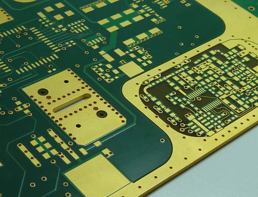
OSP PCB surface finish (Organic Solderability Preservative) is a cost-effective alternative to traditional coatings like HASL and ENIG. Unlike metallic finishes, OSP uses a water-based organic compound to protect copper pads from oxidation. Today, we will break down its process, performance, and best-use scenarios. In PCB manufacturing, the OSP process has become a mainstream choice for sectors such as consumer electronics and industrial control systems, thanks to its advantages: environmental friendliness, low cost, and suitability for fine-pitch circuitry. For PCB manufacturers, mastering the fundamentals of the OSP process is essential to producing boards that meet customer specifications and ensure reliable soldering performance.
osp pcb surface finish
Understanding the core principle of the PCB OSP process: It involves the chemical deposition of a uniform, dense organic protective film onto the bare copper surface of the PCB. This film acts as a barrier against air and moisture, preventing copper oxidation; yet, during soldering, it rapidly decomposes to expose clean copper for bonding with the solder. Simply put, the OSP film acts as a "temporary protective coat"—safeguarding the copper foil during production, storage, and transport, while "automatically shedding" during soldering without compromising solder joint quality.
OSP PCB Surface Finish Process Flow:
PCB Cleaning
Cleaning the circuit board removes contaminants such as oil, fingerprints, and oxidation layers from the copper surface. Creating a high-quality surface is crucial; incomplete cleaning can lead to uneven surface coatings in subsequent steps due to chemical reactions with residual contaminants. Chemical tanks should be inspected and cleaned regularly to maintain the proper concentration of chemical agents during the cleaning process.
Micro-etching Enhancement
During this stage, a small amount of the copper surface is micro-etched to prevent oxidation caused by environmental exposure. Removing a controlled amount of copper improves the bonding between the copper and the OSP solution. To ensure a uniform finish across the board, the etching rate is controlled to regulate coating thickness, resulting in a consistent coating and a smoother surface finish.
Acid Pickling
The circuit board is then rinsed in an acidic solution, such as sulfuric acid, to ensure the effectiveness and reliability of the OSP coating.
OSP Process
The OSP solution is applied to the circuit board, followed by an acidic rinse.
Deionized (DI) Water Rinse
Ions are added to the OSP solution to facilitate their removal during the soldering process. Rinsing the board with deionized water helps prevent the introduction of contaminants to the surface that could compromise OSP performance.
Drying
Finally, the boards are dried to remove excess moisture and maintain a uniform coating thickness.
Characteristics of OSP PCB Surface Finish
Cost-Effective: OSP surface finish is significantly less expensive than other finishes on the market, making it a preferred choice for PCB designers and manufacturers working within budget constraints.
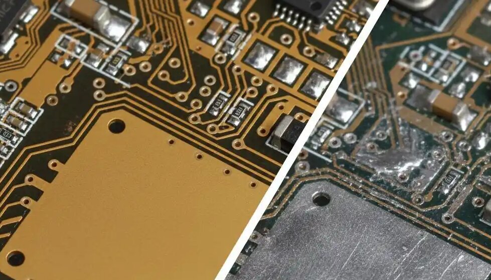
Shelf Life: Because the OSP coating on the copper surface is extremely thin, it degrades over time when exposed to harsh environmental conditions, such as fluctuations in temperature and humidity. Proper storage is essential to ensure optimal board performance during component assembly and soldering.
Environmentally Friendly: As the process involves no toxic chemicals, the coating is RoHS compliant and considered environmentally friendly.
Thin Coating: Unlike other finishes, OSP provides an ultra-thin coating that minimizes impact on the overall PCB thickness while maintaining excellent performance and solderability.
Superior Solderability: OSP coatings offer excellent solderability, ensuring a strong bond between components and copper pads during assembly. The flat OSP surface allows solder paste to conform perfectly to the pads, facilitating precise component alignment and ensuring durable solder joints during reflow soldering.
osp pcb surface finish
Packaging and Storage
OSP is a thin organic coating on the PCB surface. Prolonged exposure to high temperatures and humidity can cause oxidation and reduced solderability. Additionally, the reflow soldering process thins the organic layer, making the underlying copper foil susceptible to oxidation. Therefore, the storage and handling of OSP PCBs and SMT semi-finished products should adhere to the following principles:
OSP PCBs should be vacuum-packed with desiccant and humidity indicator cards included in the package. Interleaving paper must be used during transport and storage to prevent friction from damaging the OSP surface.
Avoid exposure to direct sunlight and maintain proper storage conditions: relative humidity of 30–70% and temperature of 15–30°C; the shelf life is at least 6 months.
On the SMT production line, always check the humidity indicator card after powering up and ensure the boards remain in the process flow for no more than 12 hours. Do not open a large number of packages at once; leaving opened packages unused or allowing boards to sit idle at a machine for extended periods can easily lead to issues. Proceed to the reflow oven as soon as possible after printing; do not let the boards sit, as solder paste is highly corrosive to the OSP coating.
Maintain a suitable workshop environment: relative humidity of 40–60% and temperature of 22–27°C. During production, avoid direct hand contact with the PCB surface to prevent oxidation caused by sweat contamination.
Second-side SMT assembly must be completed within 24 hours of the first-side assembly.
DIP assembly should be completed as soon as possible (within a maximum of 36 hours) after SMT processing.
OSP PCBs must not be baked, as high-temperature baking can degrade the OSP coating's color; if bare boards exceed their shelf life, they can be returned to the OSP manufacturer for rework.
For PCB manufacturers, mastering the fundamentals of the OSP PCB surface finish process enables a better balance between product performance and cost. As the demand for fine-line, high-reliability PCBs grows with the rise of 5G and AIoT devices, the OSP pcb surface finish process has become an essential skill; early mastery of this technology provides a significant competitive advantage in the market.