A Trustworthy PCB and Electronic Manufacturing Enterprise! Contact Us



1. PCB Damage; Repair Overview
PCB damage frequently occurs during mass production, assembly, testing and end-user application. Most minor and moderate PCB defects are repairable with standard tools and professional techniques, eliminating the need for full board scrapping. Proper PCB repair helps manufacturers cut production costs, boost finished product yield, and resolve equipment malfunctions caused by circuit board abnormalities.
This guide covers practical, industry-proven fix solutions for the most common PCB issues, including lifted solder pads, broken traces, short circuits, cold solder joints, board burnout and solder mask damage.
2. Common PCB Damages and Professional Repair Steps
2.1 Lifted / Falling Off Solder Pads
Cause: Excessive soldering temperature, repeated rework, improper desoldering, or external pulling force during wire assembly. This is one of the most prevalent defects in secondary PCB
processing.
Fix Steps:
Clean residual solder and dust from the PCB surface.
Gently polish the exposed copper trace to reveal a clean conductive layer.
Bridge the broken circuit with conductive silver glue or fine solder wire.
Secure and insulate the repaired area with UV curing glue.
Once fully cured, re-solder the components or wires to complete the repair.
2.2 Broken PCB Trace / Open Circuit
Cause: Board bending, mechanical scratches, long-term oxidation and corrosion, or overcurrent that burns out local copper traces.
Fix Steps:
Locate the exact breakpoint using a multimeter continuity test.
Strip the solder mask on both sides of the broken trace and tin the exposed copper.
Bridge the gap with fine solder wire and weld firmly.
Apply insulating paint to the repaired area to prevent oxidation and adjacent short circuits.
2.3 PCB Short Circuit
Cause: Solder bridging between adjacent pins or traces, residual flux and solder paste, board surface carbonization, or leftover conductive debris on the PCB.
Power off the device and discharge all electricity completely.
Identify the short-circuit area with a multimeter.
Remove excess solder using desoldering braid. Clear carbonized substrate and conductive impurities.
Clean the PCB surface with alcohol and dry thoroughly. Test circuit continuity before powering the device on again.
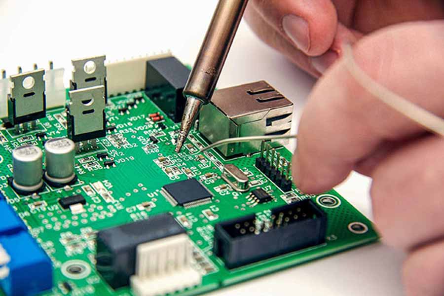
2.4 Cold & Virtual Solder Joints
Cause: Unstable soldering temperature, insufficient solder volume, oxidized component pins or PCB pads, and overly fast production cycles leading to incomplete soldering.
Fix Steps:
Reheat and rework the faulty solder joints with a constant-temperature soldering iron.
Add adequate solder to fill gaps and form full, bright joints.
Remove pin oxidation with flux. Ensure no pores or gaps remain.
Verify stable electrical conduction after cooling down.
2.5 Local PCB Board Burnout
Cause: Current overload, positive-negative pole reversal, circuit overloading, or component breakdown that generates extreme local high temperature and burns the board.
Fix Steps:
Completely remove carbonized PCB substrate to eliminate hidden leakage current risks.
Replace all burned and damaged components.
Rebuild broken circuits with fine jumper wires.
Apply full insulation treatment to the repaired area.
Conduct aging tests to confirm long-term circuit stability.
2.6 Surface Scratch & Solder Mask Damage
Cause: Mechanical friction during production, packaging and transportation, which exposes bare copper traces and leads to oxidation and short-circuit risks.
Fix Steps:
Clean the scratched area with alcohol to remove dust and debris.
Apply a thin, uniform layer of insulating solder mask oil.
Cure the coating under UV light to form a protective film for exposed copper traces, preventing oxidation and circuit faults.
3. PCB Repair Taboos & Critical Precautions
Blind and non-standard repair operations often cause secondary damage, resulting in full board scrapping.
All PCB repair work must comply with the following rules:
- No Live Operation: All soldering and repair work must be performed with the device powered off and fully discharged.
- Strict Temperature Control: Maintain soldering temperature between 300-350℃ to avoid substrate burning and further pad peeling.
- Avoid Over-Polishing: Excessive polishing thins copper traces, reduces current-carrying capacity and leaves hidden circuit faults.
- Isolate Short Circuits First: Never repeatedly power on a short-circuited board, which will expand the burned area and worsen damage.
- Post-Repair Insulation: All rebuilt traces and exposed solder joints must be fully insulated for subsequent assembly and long-term use.
4. Daily Prevention Tips to Reduce PCB Damage
Most PCB defects stem from irregular operation and inadequate protection. Standardized processing and handling can significantly lower defect rates and reduce rework costs:
- Avoid excessive bending, squeezing and violent friction during PCB assembly and packaging.
- Standardize soldering temperature and operation duration to prevent high-temperature pad peeling.
- Complete strict current and voltage testing before mass production to avoid overload burnout.
- Maintain a dust-free production environment to prevent conductive debris-induced short circuits.
5. Conclusion
Common PCB damages including lifted pads, broken traces, short circuits and virtual solder joints are all repairable with standardized, professional operations. Mastering scientific PCB repair techniques effectively reduces scrap loss, improves production efficiency and ensures product stability. For industrial mass production, standardized operation and proactive prevention are far more valuable than post-damage repair.