A Trustworthy PCB and Electronic Manufacturing Enterprise! Contact Us


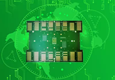
IC board design can be found in most electronic devices. An integrated circuit (IC) is a small chip containing numerous electronic components. ICs can perform a wide range of tasks, such as storing data or controlling signals. They are used in computers, mobile phones, and even toys. Understanding integrated circuits helps in grasping how these devices function. Each IC features a unique design tailored to ensure proper operation. Integrated circuit chips are present in virtually all modern devices; their design dictates their operating speed and overall performance.
The Role of ICs on PCBs
Core Functions
Think of an integrated circuit (IC) as the "brain" of an electronic device. ICs govern the transmission of signals and the device's responses. They are used to process data, store information, and manage timing. Many devices rely on ICs to execute tasks quickly and accurately. ICs can switch signals, amplify sound, and even perform mathematical calculations—making your devices smarter and faster. They are essential for ensuring that everything runs smoothly.
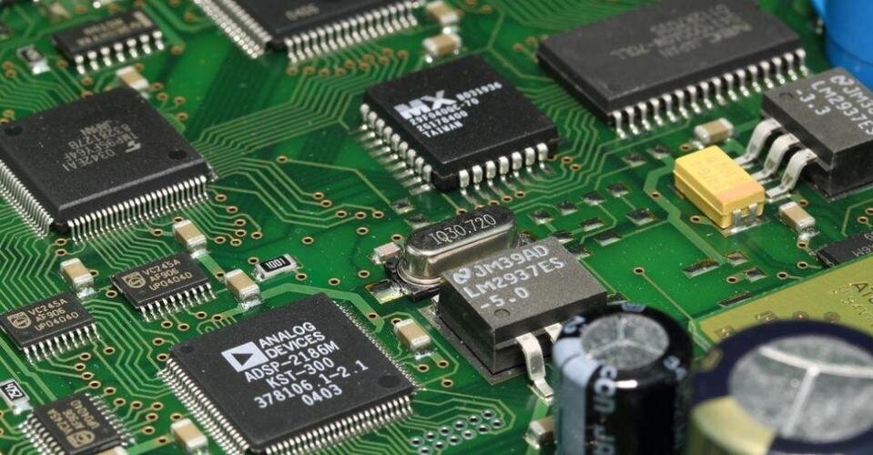
IC board
Common IC Components
Ceramics
Ceramic components are widely used on integrated circuit boards, particularly in devices measuring 5 mm or larger. They help reduce the overall size and weight of a product while ensuring efficient operation. Furthermore, ceramics possess excellent thermal properties; their low thermal conductivity aids in heat dissipation. Research has shown that applying a thin layer of ceramic fibers to the back of a PCBA (printed circuit board assembly) can effectively inhibit heat transfer. Consequently, ceramics are an ideal material for enhancing the energy efficiency and temperature control of PCBs.
Ultra-Thin Micro-Metal Packages
In space-constrained circuits, ultra-thin micro-metal (ML) packaged chips are an ideal choice for integrated circuits (ICs). These chips can be connected to the circuit via leads or fine bond wires, making them suitable for a variety of applications. The ML series is particularly well-suited for power amplifiers, voltage regulators, DC-DC converters, and oscillators, offering benefits such as low forward voltage, high efficiency, and a long operational lifespan. Their compact size allows for space-saving designs without compromising high-performance capabilities. SMD (Surface-Mount Devices)
These miniature components are mounted directly onto the surface of a printed circuit board (PCB) without the need for through-hole soldering. They are widely used in various digital circuits—particularly for logic and memory functions found in numerous electronic devices. By eliminating the need for the drilled holes required by conventional components, SMDs help save space and reduce assembly effort, facilitating the creation of compact and efficient circuit layouts. Because SMDs allow for a dense arrangement of components, they are essential in modern electronics for making devices smaller, lighter, and more efficient.
Connectors
Serving as the physical interface between a circuit board and external systems, connectors are primarily responsible for stable power transmission and signal exchange. Key design considerations include contact resistance, mating cycle durability (lifespan), and resistance to external mechanical stress.
Discrete Semiconductors
Unlike highly integrated ICs, these components—primarily diodes, transistors, and MOSFETs—act as "switches" or "valves" within a circuit. They are designed to handle high currents and high voltages, or to perform signal amplification, serving as a critical bridge between the main controller and external loads.
Resistors, Capacitors, and Inductors (Passive Components)
These are the most fundamental passive components. While they lack computational capabilities, they are used in the greatest quantities. Their primary functions include regulating voltage, filtering out noise, and storing electrical energy. Positioned closely around chips, they ensure a clean and stable operating environment.
Protection and Thermal Management Components
This category includes TVS (Transient Voltage Suppressor) diodes, fuses, and metal heatsinks. The former act as "fuses" for the circuit, absorbing sudden electrostatic discharges or voltage surges; the latter are designed for high-power-consumption chips, increasing surface area to accelerate heat dissipation.
To design or repair electronic products, one must understand the principles behind integrated circuit board design. A complete design process typically follows a sequential workflow: component selection, schematic design, PCB layout and routing, and simulation-based verification. The process begins with selecting the appropriate integrated circuits (ICs) for the project, taking into account their functionality and compatibility with other components. Next, a circuit board layout is drafted to determine the placement of each IC. Following the use of software tools to assist in the design, a final review is conducted to ensure that all IC connections are correct. A well-executed design is essential for the smooth operation of the device.
I. Schematic Design: Defining Circuit Connections
The first step in the design process is to connect the ic board to other components within the circuit. This involves defining how signals are transmitted across the PCB and establishing the locations for power supply connections. Circuit schematics are typically created using computer-aided design (CAD) software, such as Eagle, KiCad, or Altium Designer. Once the schematic is complete, the design process moves on to the physical mapping stage.
II. PCB Layout Design: From Schematic to Physical Layout
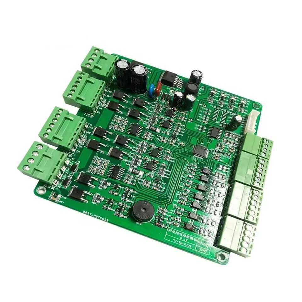
After the schematic is finalized, the design proceeds to physical mapping—converting the schematic into a detailed layout that specifies the position of each component on the board, as well as the routing of the copper traces or wires that connect them. This stage involves three key tasks:
Layer Configuration: Modern circuits are often complex and may require multi-layer PCBs. While simple IC-based designs might function on a single-layer board, most contemporary circuits require at least two layers to manage various signals, power supplies, and ground connections. For smaller IC-based boards—such as those using a 555 timer—a two-layer PCB is generally sufficient; however, more complex ICs, like the STM32, require multi-layer boards.
Component Placement: The strategic placement of components on a PCB determines its performance. Typically, the IC is positioned at the center of the board, with peripheral components arranged nearby. Components that need to communicate or function together should be placed as close to one another as possible to minimize signal transmission distances and reduce the risk of unwanted noise interference.
Trace Routing: Routing refers to the process of designing the copper paths that connect individual components. To prevent signal degradation or coupled noise within the PCB, this process must adhere to specific design rules.
III. Simulation and Verification: Ensuring Design Compliance with Standards
Once layout and routing are complete—and before moving to the manufacturing phase—it is essential to perform PCB simulation. This process confirms whether the circuit board meets specified performance standards. Every integrated circuit (IC) has defined operating voltage, current, and temperature ratings; during simulation, these parameters must be verified against the values provided in the component’s datasheet. Furthermore, the design should be validated and optimized across several specialized dimensions:
Signal Integrity (SI): Managing high-speed signals (such as those on a DDR memory bus) by controlling signal distortion and addressing factors like impedance, reflections, and crosstalk.
Power Integrity (PI): Designing a stable and "clean" Power Delivery Network (PDN) to prevent operational failures when powering ICs (as power integrity issues can also degrade the performance of connected circuitry). This involves the strategic placement of decoupling capacitors and the optimization of high-current paths to minimize voltage drops.
Thermal Management: Incorporating copper pours and thermal vias for high-power ICs to maximize heat dissipation, thereby preventing thermal throttling and catastrophic thermal failure.
Design for Manufacturing (DFM): Accounting for the physical constraints of PCB fabrication and assembly to ensure the design can be manufactured reliably with a high yield.
Ultimately, a high-performance, reliable circuit board is the result of an interconnected design process encompassing component selection, layout, routing, and verification. While the circuit board design establishes the product's upper performance limit, the manufacturing process sets the lower limit—even the best design requires capable manufacturing processes to be successfully realized. If you are working on an ic board design, we provide comprehensive support—from design reviews and DFM checks to prototyping and mass production—helping you achieve higher yields and faster time-to-market.