A Trustworthy PCB and Electronic Manufacturing Enterprise! Contact Us


The IC substrate is mainly used to carry ICs (Integrated Circuit), with internal wiring to conduct signals between chips and circuit boards. In addition to its carrying function, the IC substrate also has additional functions such as protecting circuits, and dedicated lines, designing heat dissipation pathways, and establishing modular standards for components.
IC substrates are developed based on HDI circuit boards, and there is a certain correlation between the two. However, the technological threshold of IC substrates is much higher than that of HDI circuit boards and ordinary PCB circuit boards. IC substrates can be understood as high-end PCBs, which have characteristics such as high density, high precision, high number of pins, high performance, miniaturization, and thinness. They require higher technical parameters, especially the core line width/line spacing parameters.
The IC substrate is a key material for transistor packaging. The integrated circuit industry chain is divided into three stages: chip design, wafer manufacturing, and packaging testing. Packaging not only serves to protect the chip and enhance thermal conductivity, but also connects external circuits with the interior of the chip to achieve the function of fixing the chip. IC Package Substrate (IC Package Substrate, also known as Package Substrate) is a key carrier in the packaging testing process, used to establish signal connections between ICs and PCBs. IC Substrates can also play a role in protecting circuits, fixing circuits, and dissipating waste heat.
IC substrates are applied in mainstream packaging technologies. The packaging of transistor chips has undergone several generations of changes, classified by packaging technology into DIP packaging (dual inline packaging technology), SOP packaging (small form factor packaging), QFP packaging (small square plane packaging), PGA packaging (pin grid array packaging technology), BGA packaging (solder ball array packaging), and SIP packaging (system level packaging). The iteration and upgrading of technology have enabled the current packaging area and chip area to approach 1.
Taking BGA (Ball grid array) packaging as an example, it is a high-density packaging technology that distinguishes it from other packaging chip pins distributed around the chip. BGA pins are located on the bottom surface of the packaging, increasing the spacing between I/O terminals and the number of I/Os that can be accommodated. BGA packaging has become one of the mainstream packaging technologies due to its high yield, good electrical characteristics, and suitability for high-frequency circuits. On the basis of BGA, high-density IC packaging pipelines such as CSP, MCM, and SIP have gradually emerged. Advanced packaging technology is more in line with the characteristics of miniaturization, complexity, and integration of integrated circuits. IC substrates are widely used in mainstream packaging technologies due to their high precision, high density, miniaturization, and thinness.
There are various types of IC substrates and they are widely used. It can be classified according to the packaging pipeline, processing material, and application field.
1. According to the classification of packaging pipelines, IC substrates are divided into BGA packaging substrates, CSP packaging substrates, FC packaging substrates, and MCM packaging substrates.
2. According to the classification of packaging materials, IC substrates are divided into hard packaging substrates, flexible packaging substrates, and ceramic packaging substrates. The rigid packaging substrate is mainly made of BT resin or ABF resin, with a CTE (coefficient of thermal expansion) of approximately 13 to 17 ppm/° C. The flexible packaging substrate is mainly made of PI or PE resin, with a CTE of approximately 13 to 27 ppm/° C. Ceramic packaging substrates are mainly made of ceramic materials, such as aluminum oxide, aluminum nitride, or silicon carbide, which have relatively low CTE, about 6 to 8 ppm/° C.
3. According to the classification of application fields, IC substrates are divided into storage chip packaging substrates, microelectromechanical system packaging substrates, RF module packaging substrates, processor chip packaging substrates, and high-speed communication packaging substrates.

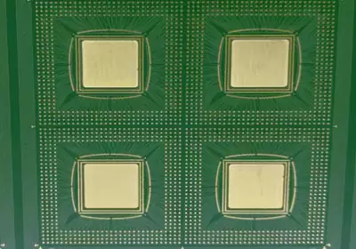
BGA packaging substrate
The requirements for IC substrates in terms of parameters are much higher than those of general PCBs and HDIs. Based on line width/line spacing, conventional IC substrate products can reach up to 20 μ M/20 μ m. The line width/spacing of high-end IC substrates will be reduced to 10 μ M/10 μ m. 5 μ M/5 μ m. And for ordinary performance PCB products, the line width/line spacing is 50 μ M/50 μ Above m.
There are two types of IC substrate manufacturing processes, namely SAP (semi additive method) and MSAP (improved semi additive method), used for producing line width/line spacing less than 25 μ m. Products with more complex process flow. The production principles of SAP and MSAP are similar, briefly described as coating a thin copper layer on the substrate, followed by graphic design, electroplating the required thickness of copper layer, and finally removing the seed copper layer. The basic difference between the two process flows is the thickness of the seed copper layer. The SAP process starts with a thin layer of chemically plated copper coating (less than 1.5um), while MSAP starts with a thin layer of laminated copper foil (greater than 1.5mum).
The subtractive method is a PCB circuit board manufacturing method, which is briefly described as electroplating a layer of copper on the entire board of the copper-clad board, protecting the circuit and through holes, etching off unnecessary copper sheets, and leaving copper in the circuit and through holes. The most obvious drawback of the reduction method is its high lateral corrosion, which means that the copper layer will also be etched on the side during the downward etching process, limiting the precision of the reduction method. Therefore, the minimum line width/spacing of the subtraction method can only reach 50 μ m. When line width/line spacing<50 μ When the yield is too low, the subtraction method cannot be used.
There are multiple technological difficulties in the production process of IC substrates, which are reflected in five aspects: material expansion and contraction control, graphic formation, copper plating, solder mask process, and surface treatment throughout the entire process.