Impedance Calculation
The following is an example of an eight-layer board stack as shown in Figure 1 to introduce the relevant impedance calculation method.
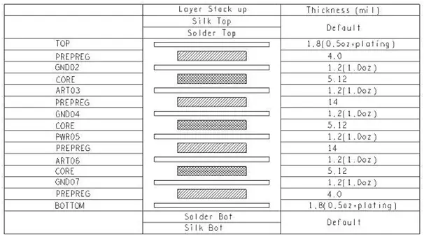
Figure 1-8 layers of boards
Microstrip Impedance Calculation
1, The surface layer (Top/Bot layer) refers to the second layer, single-ended impedance CoatedMicrostrip1B model, single-ended 50 ohm impedance calculation method as shown in Figure 2, and finally get the surface layer 50 ohm single-ended line width of 6mil.
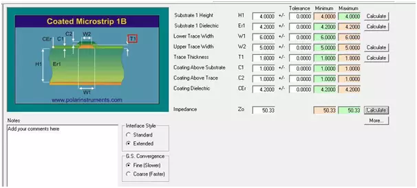
Fig. 2 - Calculation of Single-Ended Impedance of Top/Bot Layer
2, The surface layer differential impedance selected Edge-CoupledCoated Microstrip1B model, differential 100 ohm impedance calculation as shown in Figure 3, the final obtained surface layer 100 ohm differential line width line spacing is 4.7/8 mil.
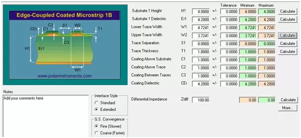
Figure 3 - Differential Impedance Calculation for Top/Bot Layer
3. Calculation of the 50 ohm impedance of the RF signal in the top/bot layer:
Because the RF signal has to have a wide enough line width, if the impedance remains unchanged, increasing the line width will add the distance from the impedance line to the reference layer, so the 50 ohm RF signal has to be a spaced reference, that is, the third layer, and the impedance model is chosen to be CoatedMicrostrip2B. The impedance calculation method is as shown in Fig. 4, and the line width of the 50 ohm RF signal in the top layer is 15.7 mil. The line width of the 50 ohm RF signal on the surface layer is 15.7 mil.
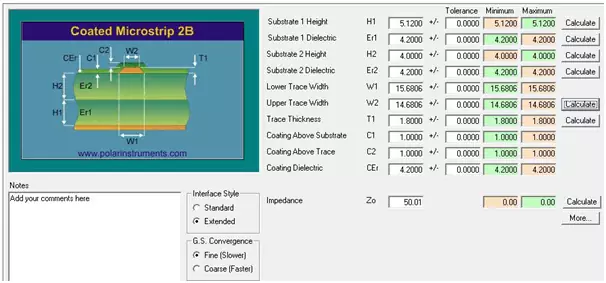
Figure 4 - Surface 50 Ohm RF Signal Impedance Calculation
4, Description of impedance calculation parameters of microstrip line:
H1 is the thickness of the surface layer to the dielectric of the reference layer, excluding the copper thickness of the reference layer;
C1, C2, C3 is the thickness of the green oil, generally the thickness of the green oil is around 0.5mil~1mil, so it is good to keep the default, and its thickness does not have a great influence on the impedance;
The thickness of T1 is generally the thickness of the surface layer base copper plus the thickness of plating, 1.8mil for 0.5OZ (base copper thickness) + Plating results;
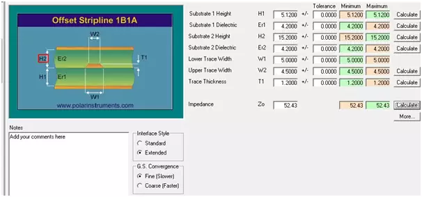
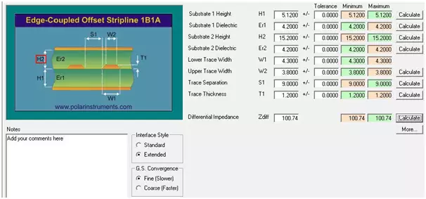
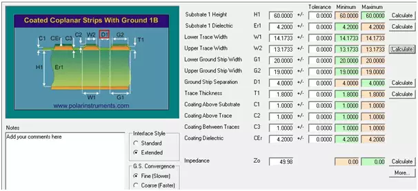
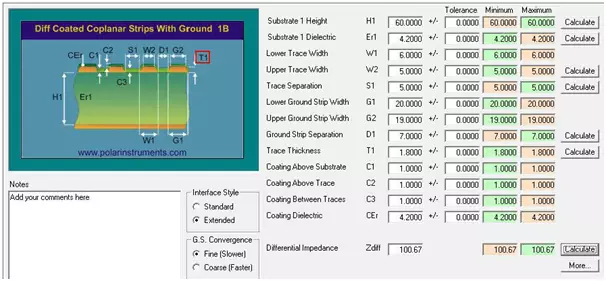
Generally W1 is the width of the line on the board, due to the trapezoidal shape of the processed line, so W2 Stripline impedance calculation 1, Strip line (Art03 and Art06 layers) inner single-ended impedance using Offeset Stripline1B1A model, 50 ohm impedance calculation method as shown in Figure 5, the calculated inner 50 ohm single-ended line width is 5mil. Figure 5 - Internal 50 Ohm Single-Ended Impedance Calculation 2, Stripline (Art03 and Art06 layers) inner layer differential impedance using Edge-Coupled Offeset Stripline model 1B1A, 100 differential ohm impedance calculation method as shown in Fig. 6, the calculated inner layer of 100 ohm differential line width spacing is 4.3/9mil. Figure 6 - Internal 100 Ohm Differential Impedance Calculation 3. The parameters of impedance calculation for strip line are explained: H1 is the thickness of core between the lead wire and the reference layer, and H2 is the thickness of pp between the lead wire and the reference layer (considering the situation of pp flow glue). As shown in Figures 7-14 and 7-15, the impedance calculation diagram shows that, for example, in the case of ART03, H1 is the thickness of the dielectric between GND02 and ART03, and H2 is the thickness of the dielectric between GND04 and ART03 plus the thickness of copper, so the value of H2 should be 14mil+1.2mil=15.2mil. H2 is the dielectric thickness between GND04 and ART03 plus the copper thickness, so the value of H2 should be 14mil+1.2mil=15.2mil; When the dielectric between Er1 and Er2 is different, the corresponding dielectric constant can be filled in; The thickness of T1 is generally the thickness of the inner layer of copper; when it is HDI board, you need to pay attention to whether the inner layer is plated or not, if it is plated, you need to add the thickness of the plating. Coplanar Waveguide Impedance Calculation The above is a common impedance calculation, however, some PCB boards are thicker and have fewer layers, so there is no way to calculate the specific parameters of the impedance line by using the above method. At this time, we have to consider the Co-planar Waveguide model, which is a model where the signal line takes reference of the ground line beside it to do the impedance, and it is generally used more in double-panel applications. 1, Single-terminal 50 ohm, select Coated Coplanar Strips With Ground1B model, the impedance calculation method is shown in Fig. 7, the calculation structure for the impedance line width of 14mil, the impedance line to the ground distance of 4mil, the width of the ground line is 20mil. Figure 7-50 Ohm coplanar waveguide impedance model calculation 2, differential 100 ohms, select Diff Coated Coplanar Strips With Ground1B, the impedance calculation method is shown in Figure 8, the calculation results in 100 ohms differential line width line spacing is 6/5mil, the distance from the differential line to the ground line is 7mil, the ground line width is 20mil. Figure 8-100 Ohm Differential Coplanar Waveguide Impedance Model Calculation 3. Parameters of coplanar waveguide impedance calculation: H1 is the thickness of the dielectric from the impedance line to the nearest reference layer; G1 and G2 are the widths of the accompanying ground, generally the larger the better; D1 is the distance between the impedance line and the accompanying ground. 4, A few notes on impedance calculation Line width is preferred to be wide rather than thin. Because we know that there is a fine limit in the process, and there is no limit for wide. If the board factory to adjust the impedance to adjust the line width of fine and encountered the fine limit, it will be a problem, either new costs, or relax the impedance control, or modify the design ... So in the calculation of the relative width of the impedance implies that the target impedance is slightly lower, for example, 50 ohms, we calculate to 49 ohms can be, as far as possible, do not calculate to 51 ohms. There is an overall trend. We may have more than one impedance control target in our design, so let's go big or small, not big for 100 ohms and small for 90 ohms. Consider the copper residual rate and the amount of glue flow. When one or both sides of the semi-cured sheet are etched lines, the adhesive will be pressed to fill the gaps in the etching process, so the thickness of the adhesive between the two layers will be reduced, the lower the residual copper rate, the more filler, the less left. So if you need two layers of semi-cured sheet thickness is 5mil, according to the copper residual rate to choose a slightly thicker semi-cured sheet (4) Specify the type of glass cloth and the amount of glue. Looked at the plate datasheet know different glass cloth, different glue content of the half-cured sheet or core plate node coefficient is different, even if it is about the same height may be 3.5 and 4 difference, this difference can cause a single line impedance of about 3 ohm change. In addition, the glass fibre effect and glass cloth window size is closely related, if you are 10Gbps or more high-speed design, and your stack does not specify the data, the board factory used a single 1080 data, then there may be signal integrity problems. Communicate more with circuit board manufacturers Of course, the copper residual rate and the amount of adhesive flow will sometimes be calculated incorrectly, the dielectric coefficient of the new material is sometimes inconsistent with the nominal, and some glass cloth board manufacturers do not have spare material, etc. will cause the design of the stack can not be realised or delayed delivery. When these situations occur, the best way is to let the board factory at the beginning of the design according to the designer's requirements, according to their experience in designing a stack, after a number of communication and confirmation, so that up to a few back and forth can get the ideal stack, to facilitate the subsequent impedance calculation and circuit design.