A Trustworthy PCB and Electronic Manufacturing Enterprise! Contact Us



Electronic design and PCB manufacturing face widespread interconnection bottlenecks amid device miniaturization upgrades. PCB board pin connectors serve as core precision interconnect parts, effectively solving common pain points including bulky traditional connectors, unstable wiring and poor signal performance, perfectly fitting modern high-density, high-speed circuit design demands.
Against this industry backdrop, these high-precision pin connection components have become indispensable for modern electronic interconnection systems. Tiny yet exquisitely manufactured, they act as reliable bridging units between electronic parts, circuit boards and functional modules. Featuring compact structure, stable conduction, flexible layout and simple assembly and maintenance, they have gradually replaced outdated connection methods and become a mainstream option for electronic research, mass production and product iteration worldwide.
Many engineering practitioners tend to overlook the practical value of these customized connecting parts, simply treating them as ordinary metal accessories. In reality, the whole circuit conduction, signal transmission and module linkage of electronic devices rely heavily on their precise docking and stable conduction. They not only build steady electrical pathways for power and data transfer but also deliver solid mechanical support for modular circuit structures, underpinning the long-term stable operation of electronic equipment.
Core Value of PCB Board Pin Connectors in Electronic Design
Traditional connection methods have inherent flaws that restrict product upgrading and production efficiency. Standard traditional connectors feature fixed shapes and pin counts, which occupy valuable PCB layout space and limit circuit expansion capabilities. Manual scattered wiring leads to disordered circuit distribution, weak anti-vibration and anti-interference performance, and frequent open circuits or poor contact after long-term equipment operation. In addition, traditional connection structures are mostly fixed and non-detachable, requiring overall component replacement for circuit modification or product iteration, resulting in high time and material costs.
Professional-grade PCB board pin connectors perfectly solve all the above industry pain points. Adopting high-precision formed metal contacts and insulated structural design, they form meshed matching connections with supporting sockets. This structural design ensures continuous and stable electrical conduction while greatly enhancing the mechanical stability of the entire connection assembly. Whether for compact micro-layouts with limited space, high-density multi-channel signal transmission, or complex working conditions involving high and low temperature alternation, mechanical vibration, and environmental corrosion, these connectors maintain extremely low signal loss, strong anti-interference ability, and long-term durable performance.
They also bring unique advantages for industrial mass production and later maintenance. Designed with low insertion force, PCB board pin connectors support efficient batch assembly without complex processing procedures. For equipment inspection, module replacement, and product function upgrades, the detachable connection structure avoids modifying the original PCB substrate, greatly reducing post-production maintenance costs and improving overall production and operation efficiency. These comprehensive advantages make them essential accessories for civilian consumer electronics, industrial automation, automotive electronics, medical devices, and aerospace precision equipment.
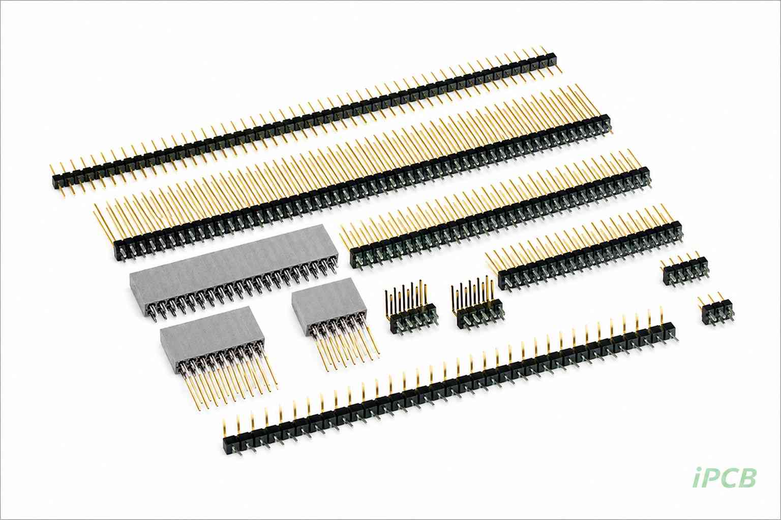
Main Types and Styles of PCB Board Pin Connectors
PCB board pin connectors feature diverse categories and rich structural styles to adapt to differentiated circuit scenarios, assembly processes, and space constraints. Improper model selection easily causes circuit instability, assembly failure, and signal transmission errors. Based on functional purposes and structural forms, mainstream connector types are systematically sorted below to help engineers select targeted models and avoid design pitfalls.
Classification by Functional Purpose (Covers Most Circuit Scenarios)
1. Terminal Pins – First Choice for Discrete and Custom Wiring
Terminal pins are independent single PCB pins without integrated plastic bases, supporting flexible independent installation according to actual circuit requirements. They are highly adaptable for scattered circuit connection points, customized PCB design, and non-standard small-scale equipment wiring. Occupying no redundant board space, terminal pins solve the interconnection pain points of discrete circuit points and are universal accessories for non-standard electronic design.
2. Pin Headers – Core Standard for Mass Production
As the most widely used and highly standardized PCB connectors in the electronics industry, pin headers integrate multiple male pins into a molded plastic base with neat and uniform arrangement. Fully compatible with automated SMT assembly processes, they are mainly applied to board-to-board fixed connection, functional module docking, and circuit expansion. Almost all standard PCBs for consumer electronics, industrial control, and communication equipment adopt pin headers as the basic interconnection standard for mass production.
3. Female Headers – Detachable Interconnection Matching Accessories
Female headers are supporting socket contacts used in pair with pin headers. The precise meshing structure forms a fully detachable board-to-board connection system, completely different from traditional non-detachable soldered connections. This combination supports free disassembly and debugging of circuit boards and functional modules, greatly facilitating product R&D testing, post-maintenance replacement, and equipment iterative upgrades. It is the core matching solution for modular electronic products requiring repeated debugging and assembly.
4. Jumper Pins – Special Tools for Testing and Debugging
Jumper pins are miniature precision connectors focused on flexible circuit switching. They are widely used for circuit bridging, R&D debugging, mass production testing, and circuit on-off switching. Engineers can quickly adjust circuit logic through jumper pins without re-soldering or modifying PCB substrates, significantly improving the efficiency of single-chip development, circuit testing, and equipment function calibration.
Classification by Structural Style (Precise Adaptation to Process and Space)
To meet diverse manufacturing processes, space limitations, and signal transmission requirements, PCB board pin connectors have derived multiple refined structural styles, each corresponding to exclusive application scenarios:
1. Single-ended / Double-ended Connection
Single-ended pins support one-sided circuit connection, suitable for single-sided board fixing and one-way module docking. Double-ended pins realize double-sided cross-board interconnection, adapting to double-layer PCB penetration connection and cross-module circuit conduction, meeting the multi-dimensional connection needs of complex circuit structures.
2. Single-row / Double-row Arrangement
Single-row pins feature a simple structure and ultra-small footprint, ideal for low-pin-count and simple circuit connection scenarios. Double-row pins adopt parallel double-row layout, doubling the connection density per unit area, perfectly adapting to high-density multi-channel signal transmission and becoming the mainstream choice for compact high-end electronic equipment.
3. Edge-mount Type
Different from conventional centrally installed pins, edge-mount PCB pins are arranged along the edge of the circuit board, maximizing the utilization of board space. This design reserves sufficient layout areas for core components such as chips, capacitors, and sensors, fully fitting the design requirements of ultra-thin and miniaturized smart devices.
4. Functional Specialized Structures
Various customized functional pins are developed for special processes and working conditions. Nail-head pins adopt a flat-top structure to increase contact area, effectively avoiding poor contact and loose docking. Cup-shaped and slotted pins optimize welding structures to facilitate solder wire penetration and uniform solder flow, ensuring firmer welding and more stable conduction. Turret pins with shoulder structures support wire winding and test point reservation, realizing multi-functional integration. Crimp and wire-terminated pins eliminate complex welding processes and directly crimp fixed wires to simplify assembly. Shielded pins are equipped with protective structures to prevent pin deformation and oxidation during production, transportation, and assembly. Spring-loaded pins support high-frequency plugging and temporary docking, widely used in test equipment and detachable functional modules.
Mature Mounting Processes for PCB Board Pin Connectors
Unstable circuit connection, pin falling off, and low assembly efficiency are mostly caused by improper mounting process selection. PCB board pin connectors support two mature fixing methods (mechanical fixing and soldering fixing) and four universal mounting forms, which can be flexibly selected according to mechanical strength requirements, electrical performance standards, and mass production processes.
Four Core Fixing Processes
1. Press-fit Mounting – Priority for High-efficiency Mass Production
The press-fit process requires no welding or glue filling. Pins are directly pressed into PCB electroplated through holes and fixed by mechanical occlusion. The whole process involves no high-temperature thermal damage, protecting PCB substrates and surrounding precision components. Featuring fast assembly speed and high consistency, this process is highly compatible with automated mass production lines, effectively reducing labor costs and product defect rates.
2. Riveting Mounting – High-reliability Anti-vibration Solution
Pins are firmly locked on the circuit board through mechanical deformation and riveting. The fixing strength is far higher than that of ordinary welding and press-fit methods, with excellent anti-vibration and anti-impact performance. It is specially applicable to industrial automation equipment, vehicle electronics, outdoor special equipment, and other scenarios with long-term vibration and high reliability requirements, preventing pin loosening and falling off during long-term operation.
3. Crimp Mounting – Ideal for Precision Micro Devices
The controlled compression crimping process ensures uniform stress and tight connection of pins without virtual connection or loose contact. With compact structure and high assembly consistency, it perfectly meets the precision assembly requirements of micro high-precision instruments and miniature smart devices, ensuring stable connection performance of tiny circuits.
4. Soldering Mounting – Universal Stable Solution
As the most mainstream and mature mounting process in the industry, soldering fixes pins and PCB pads through tin welding. It features low contact resistance, stable electrical conduction, and strong oxidation resistance. With high process tolerance and convenient maintenance and re-welding, it is universally applicable to most civilian and industrial general equipment, with irreplaceable versatility.
Four Universal Mounting Forms
1. Surface Mount Technology (SMT)
Pins are directly soldered on PCB surface pads, compatible with automated SMT patch production. This form adapts to miniaturized and high-density circuit design and is the mainstream mounting method for current ultra-thin consumer electronic products.
2. Through-hole Mounting (THT)
Pins penetrate PCB drilling holes and are welded and fixed on the bottom of the board, with high mechanical strength and strong bearing capacity. It is suitable for high-current, high-vibration, and high-load industrial equipment scenarios, ensuring long-term structural stability.
3. Wire Mounting
Replacing traditional bare wire welding, wires are connected and fixed through clips and fixing screws. Featuring convenient disassembly and simple maintenance, it is applicable to equipment requiring frequent line adjustment and routine overhaul.
4. Free-hanging Mounting
Without fitting and fixing on the circuit board, it realizes interconnection of off-board cables and wires, adapting to special irregular wiring and long-distance cross-board connection scenarios with ultra-high compatibility.
Core Advantages of Pin Connectors Over Traditional Connectors
Traditional connectors such as circular connectors and D-sub connectors are gradually phased out in modern electronic design due to their inherent defects. In contrast, PCB board pin connectors show comprehensive competitive advantages in space utilization, layout flexibility, transformation cost, and scenario adaptability, becoming the mainstream choice for new-generation electronic interconnection.
In terms of space utilization, traditional standard connectors are bulky with fixed structures, occupying a large number of valid PCB layout areas and squeezing the installation space of core components. Their fixed and limited pin counts cannot meet the high-density multi-channel connection requirements of integrated circuits, restricting product performance expansion. These pin connectors can be arranged in high-density arrays, realizing dozens to hundreds of electrical connections in an extremely small space, greatly improving board-level interconnection density and adapting to the miniaturization and integration trend of electronic equipment.
In terms of layout flexibility and iteration cost, traditional connectors have solidified layout after installation. Product function upgrading and circuit modification require overall connector replacement, involving cumbersome processes and high material and time costs. These practical pin components support flexible grouping, position adjustment, and pin number adjustment according to design requirements, without large-scale modification of PCB substrates. This greatly simplifies product iteration processes and reduces R&D and transformation costs.
In terms of scenario adaptability and cost performance, traditional connectors are limited to fixed standard specifications and cannot adapt to non-standard and refined customized circuit scenarios. Custom pin connection components can be adjusted in size, structure, material, and plating to accurately match civilian, industrial, medical, aerospace, and other fields, covering both mass commercial products and high-precision professional equipment. Meanwhile, their modular and standardized structure reduces mass production costs, delivering far higher cost performance than traditional connectors.
Professional Selection Guide for PCB Board Pin Connectors
Improper connector selection is the main cause of equipment signal failure, heating, loosening, and oxidation faults. Reasonable selection needs comprehensive evaluation from three dimensions: physical and electrical specifications, material and plating performance, and working condition and manufacturing adaptability, ensuring matching with product design requirements.
Physical and Electrical Specification Matching
The primary selection step is to verify basic parameters to avoid assembly and electrical faults. It is necessary to accurately match pin diameter, lead size, mounting hole size, and PCB board thickness to fit the basic structure of the circuit board. Select pin shapes (round, square, rectangular) and installation directions (vertical, right-angle) according to wiring space and layout design.
In terms of electrical performance, focus on rated current, rated voltage, and transmission density. The rated current of a single ordinary pin is about 1A. For high-current power supply scenarios, multi-pin parallel connection must be adopted to share the load and prevent overheating and burnout of a single pin. Strictly check dimensional tolerances to avoid assembly misalignment and poor contact.
Contact Material and Plating Selection
Contact base materials determine the mechanical strength and conductivity of connectors. Mainstream materials include brass, bronze, copper alloy, and nickel-based alloy, which balance excellent electrical conductivity and mechanical toughness, resisting deformation and fracture during long-term operation.
Plating layers are key to improving corrosion resistance, wear resistance, and signal transmission accuracy. Tin plating is cost-effective and universally applicable, with basic oxidation resistance suitable for mass civilian consumer electronic products. Gold, silver, and palladium plating feature ultra-low signal loss, high wear resistance, and strong anti-corrosion performance, specially used for high-frequency signal transmission, precision instruments, and high-reliability special equipment to ensure long-term stable and lossless signal transmission. Nickel plating is mostly used for base protection to enhance substrate adhesion and rust resistance.
Working Condition and Manufacturing Adaptability
For special scenarios such as outdoor exposure, industrial operation, vehicle mounting, and aerospace, environmental adaptability must be prioritized. High and low temperature alternation, humidity, corrosion, and strong vibration environments require alloy base materials and precious metal plating to avoid oxidation, loosening, and open circuit faults. Meanwhile, connector selection must match automated production equipment and processes to ensure production consistency and reduce mass production defect rates.
Pin Layout Design Specifications for Engineers
Selecting high-quality connectors is only the foundation. Standardized pin layout design is the core to ensure signal integrity, suppress EMI interference, and avoid crosstalk and signal attenuation. The wiring logic of connector pins is consistent with that of PCB boards, and targeted design specifications are required for different signal types to eliminate potential circuit risks.
DC Signal Design: Stable Current and Short Circuit Prevention
The core of DC connection design is load current control and grounding stability. Limited by the single-pin current carrying capacity, multi-pin parallel connection is required for high-current power supply to avoid overload heating. Multiple voltage circuits can be arranged in a single connector to meet independent power supply requirements of multiple modules.
Grounding design is the top priority of DC circuit design. Ground pins undertake return current, and the number and layout of ground pins need reasonable planning. It is strictly forbidden to bridge different potential and different grid circuit boards through ground pins. Natural DC grounding offset exists between different grid points, and forced bridging will cause large-current short circuits, burning cables and damaging equipment, which is a forbidden operation in DC design.
Low-frequency/Low-speed Signal Design: Anti-interference and Stable Transmission
For low-speed digital signals with a rise time of 5-10ns, short-distance interconnection basically avoids crosstalk and signal reflection problems, and only one ground pin reserved in the connector can ensure stable signal transmission.
However, for connectors with large pin counts, long wiring distances, and ribbon cable connection, exposed signal pins are prone to become EMI interference sources and receive external crosstalk, resulting in signal disorder. The optimal solution is the signal-ground interleaved layout, which arranges ground pins between signal pin groups to form a natural shielding barrier and effectively suppress electromagnetic interference and crosstalk. Short-distance board-to-board connection can properly simplify ground pin configuration, while long-distance cable connection must strictly implement interleaved grounding design.
High-speed/High-frequency Signal Design: Anti-attenuation and Impedance Stabilization
GHz-level high-frequency signals and high-speed differential signals have extremely high wiring requirements. Conventional single-ended wiring is prone to impedance mismatch, signal attenuation, and differential crosstalk. The design must prioritize differential pair pin layout, with matching dedicated ground pins for each differential pair. Near-end grounding shielding eliminates crosstalk between differential pairs and optimizes impedance matching effects.
In high-frequency scenarios, more ground pins provide better shielding effects, minimizing transmission loss and stabilizing signal quality. It is worth noting that ordinary pin headers are not applicable for ultra-high frequency RF signals. U.FL coaxial connectors must be used instead. Power and low-speed signals can be wired through conventional pin connectors to realize functional partitioning and isolated anti-interference, ensuring the purity of high-frequency signals.
General Design Pitfall Avoidance
Always verify connector shields and pin definitions before pin arrangement design. Shielded connectors are prone to pin reversal errors, which will cause finished PCB docking failure and costly rework. Before selection and design, strictly refer to component datasheets and screen suitable connectors according to equipment current, bandwidth, and signal standards. Manufacturers' scenario-based product classification can also be referenced to accurately match design requirements and avoid inherent design defects.
Wide Application Scenarios of Pin Connection Components
With the comprehensive advantages of wide adaptability, high stability, cost effectiveness, easy mass production, and customizable performance, these practical pin connection parts have covered all fields of the electronic industry, serving both mass civilian consumer products and high-precision and high-reliability professional special equipment.
In the consumer electronics industry, miniature PCB board pin connectors support the lightweight and integrated design of mobile phones, tablets, wearable devices, and smart home products. In server and computing equipment, high-density pin arrays meet the requirements of multi-channel high-speed data transmission and ensure efficient equipment operation. In medical precision instruments, low-loss and corrosion-resistant pin connectors guarantee accurate detection data and stable operation of medical equipment. In test and measurement systems, the combination of jumper pins and detachable pin headers adapts to high-frequency equipment debugging, data detection, and function calibration scenarios.
In addition, they are core accessories for telecommunications infrastructure, automotive electronics, industrial automation, aerospace, and national defense equipment. Vehicle-grade pin connectors with shock resistance and high-temperature resistance adapt to complex vehicle working conditions. High-reliability pin components for industrial automation withstand long-term vibration, temperature alternation, dust, and corrosion environments. Customized high-precision PCB pin connectors ensure safe and stable operation of aerospace and defense special equipment.
From civilian mass production to high-end special scenarios, these customizable pin components can be adjusted in size, structure, material, and layout to meet differentiated demand standards, becoming indispensable basic core components in the modern electronic industry.
In the iterative upgrading of electronic technology, core components such as chips and motherboards are often focused on, while basic accessories like professional pin connectors are easily ignored. In fact, these tiny precision pins build the complete interconnection system of electronic equipment, supporting all functional operations through stable power, signal, and data transmission.
Replacing traditional backward connection schemes, high-quality pin connectors solve the core pain points of modern electronic design in space occupation, structural stability, anti-interference performance, and iteration cost. With rich product categories, mature mounting processes, and standardized design specifications, they fully adapt to R&D and mass production needs of all-industry electronic equipment.
As electronic equipment continues to upgrade toward miniaturization, high speed, integration, and high precision, PCB board pin connectors are also iterating and optimizing in material, structure, and precision. They will continue to provide stable, efficient, and low-cost interconnection solutions for modern electronic design and mass production, always maintaining their status as essential and versatile core interconnect components in the global electronic industry.