A Trustworthy PCB and Electronic Manufacturing Enterprise! Contact Us



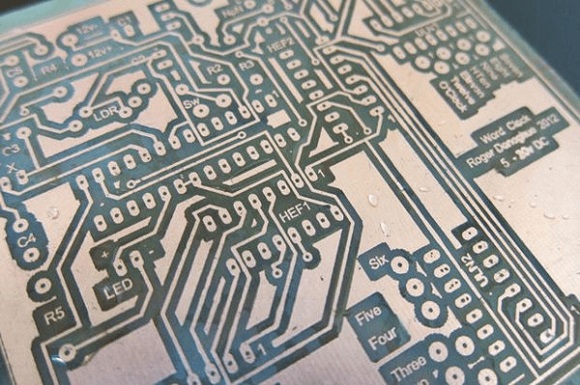
Etched circuit boards serve as the fundamental carrier for most rigid PCBs. The conductive patterns are formed through a subtractive manufacturing process, which removes excess copper foil from copper-clad laminates via chemical etching. Although this process is well-established, minor parameter fluctuations during etching can directly affect line width, impedance control, signal integrity, and final production yield. This article comprehensively explains the core etching tolerances, typical defects, key quality influencing factors, and practical DFM checklists, providing professional references for hardware engineers, purchasers, and pre-production engineering reviews.
1.Core Tolerance Requirements for Etched Circuit Boards
Tolerance control is the core standard for evaluating etched PCB quality, which is closely related to copper thickness, minimum line width, and line spacing. For standard 1oz copper (35μm base copper), the stable line width tolerance is ±0.08mm, meeting the production requirements of most conventional industrial control and consumer electronic PCBs. For 0.5oz thin copper boards or fine-line circuits below 0.1mm, the tolerance needs to be tightened to ±0.05mm, requiring high-precision exposure equipment and a stable etching production line for qualified manufacturing.
Undercut is an inherent phenomenon in chemical etching, referring to the lateral copper loss under the dry film masking area. The industry's qualified standard specifies that the undercut depth shall not exceed 10% of the copper thickness. Excessive undercut will form a tapered circuit structure (wider top and narrower bottom), reducing the effective conductive area and increasing circuit resistance. Long-term operation will cause circuit overheating and even open circuits, seriously compromising product reliability.
Higher tolerance control standards are required for impedance-controlled PCBs such as high-speed boards and RF boards. These products are extremely sensitive to impedance parameters. Slight line width deviation or excessive undercut will directly cause impedance drift, resulting in unstable signal transmission and signal distortion, making etching precision a critical control link for high-end PCB production.
2. Common Etching Defects and Root Cause Analysis
Etching defects are frequent in PCB mass production. Most quality issues stem from clear process abnormalities and can be effectively avoided through strict pre-production and in-process control.
(1). Excessive Undercut & Tapered Traces
Main causes: excessive etching time, high etchant temperature, and uneven spray pressure. Consequences: narrowed trace bottom, reduced current-carrying capacity, and unqualified product reliability.
(2). Circuit Short Circuit / Bridging
Main causes: insufficient etching, poor dry film adhesion, and surface dust or contamination. Residual copper between adjacent traces causes direct electrical short circuits, which are fatal defects leading to board scrapping.
(3). Open Circuit
Main causes: over-etching, poor lamination quality, and scratched dry film before exposure. Complete trace disconnection results in circuit failure, which is a key defect to be prevented in production.
(4). Uneven Line Width on Single Panel
Main causes: uneven etchant spray distribution and unstable conveyor speed. This inconsistency leads to ununiform circuit parameters and poor overall performance stability of the PCB.
3. Four Core Factors Affecting Etching Quality
(1).Copper Foil Thickness: Thicker copper requires longer etching time, which inevitably increases undercut degree. Therefore, ultra-fine circuits are not recommended for heavy copper boards in design optimization.
(2). Exposure and Development Quality: The precision of pattern transfer, dry film lamination, and exposure development determines the initial circuit profile. Defective imaging will cause batch abnormalities in subsequent etching processes.
(3). Etchant Parameter Stability: In mass production, the concentration, temperature, spray pressure, and circulation flow of etchant must remain stable. Parameter fluctuation is the primary cause of batch etching defects.
(4). Pre-etching Surface Treatment: Board oxidation, surface dust, and minor scratches before etching will trigger local etching anomalies, resulting in sporadic open circuits and missing copper defects.
4. Practical DFM Checklist for Etched Circuit Boards
This checklist is applicable for both designer DFM optimization and factory pre-production EQ verification to avoid potential risks:
Confirm copper thickness and matched line width tolerance before production, avoiding extreme fine-line design beyond process capability;
Adopt tightened etching tolerance for impedance-controlled and high-speed PCBs, focusing on undercut and line width consistency;
Avoid ultra-fine circuits for heavy copper boards to match actual manufacturing capacity;
Verify the consistency between Gerber files and technical specifications to prevent rework caused by parameter conflicts;
Provide line width and undercut test reports for high-reliability products including medical, automotive, and industrial control PCBs.
5. Conclusion
As a fundamental yet critical process in PCB manufacturing, etching is the main source of circuit defects, impedance deviation, and reliability risks. Stable process parameters, reasonable DFM design, and rigorous pre-production verification are essential to improve the yield rate and quality of etched circuit boards. Strict control of etching details fundamentally avoids short circuits, open circuits, excessive undercut, and signal anomalies, ensuring long-term stable performance of customized PCB products.