A Trustworthy PCB and PCBA Manufacturing Enterprise! Contact Us


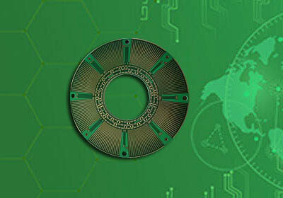

Product name: IC probe test card board
Base plate: TUC/TU872HF
Layer: 44L
Finished size: 20"*22"
Stacking: L1-L44 10mil
L1-L28 12mil
L29-L44 14mil
Surface treatment: Hard gold plating 3-15μ"
Special process: metal edging, fixed depth drilling
Product Application: Wafer Test Board
1. The probe card is the interface between the chip under test and the testing machine in wafer testing. It is mainly used to measure the electrical performance of the chip before packaging, and to screen out bad chips before packaging.
2. Integrated circuit (IC for short) is an integrated circuit that uses semiconductor manufacturing technology to manufacture many transistors, resistors, capacitors and other components on a small silicon wafer, and combines these components into a complete electronic circuit according to regulations . multilayer wiring method
3. Probe cards are divided into blade cards, cantilever cards, vertical cards, film cards and MEMS cards
4. The probe card is mainly composed of PCB, probe and functional components. Depending on the situation, there will be a need for electronic components and stiffeners. Cantilever cards also include rings, epoxy, etc.
5. Common materials for cantilever needle clamps include tungsten tungsten (W), rhenium tungsten (RW, 3% R, 97% w), beryllium copper (BeCu), paliney7 (P)
6. PCB is the carrier of needles, rings and functional components, realizing signal transmission between the needle tip and the testing machine. Its shape and size are limited by the interface method, and the materials are limited by the testing environment. The corresponding shapes are generally square and round
7. MEMS: In order to improve throughput and develop probe card technology with fine pitch and high pin count, micro-electromechanical systems; the emergence of MEMS technology has broken through the manual assembly of epoxy ring probe cards and micro-spring probes one by one Technical limitations of card welding. The high degree of automation breaks through the limitation that production costs are proportional to the number of pins, and is conducive to the production of high-pin-count probe cards. It is suitable for high pin-counts (~30K pins/card), high current and high probe compression stroke. Excellent stability and low test scratches. In other words, in extremely narrow pitch wafer testing, only very few scratches are produced, which can effectively increase durability and reduce the frequency of pin replacement.
8. The number of stuck pins of the epoxy resin cantilever probe can reach thousands, and the number of pin layers can reach 16; the distance between the cantilever pins is 30um, and the vertical pins are 40-50um.
9. Service life of cantilever probe card: 100wtd
10. Probe card storage conditions: Vacuum packaging, shipped from the factory, unused probe cards are stored in a nitrogen chamber, humidity: 25%±2

44-layer IC probe card PCB
In recent years, transistor manufacturing technology has advanced by leaps and bounds, several years ahead of the predictions of Moore's Law, and is currently moving towards below 7 nanometers. Products are required to be thin, light, and compact. ICs are becoming smaller, more powerful, and have more pins. In order to reduce the area occupied by chip packaging and improve IC performance, at this stage, flip chip (Flip Chip) pipeline packaging is generally used. Applied to graphics chips, chipsets, memories and CPUs, etc. The unit price of the above-mentioned high-end packaging pipeline is high. If the wafer can be tested before packaging and any defective products are found in the wafer, it will be marked and the marked defective products will be discarded before the subsequent packaging process, which can save unnecessary time. Packaging costs.
The probe card is a test interface that mainly tests the bare chip. It connects the test machine and the chip and tests the chip parameters by transmitting signals.
The probe is a kind of test needle used to test PCBA. The surface is gold-plated and has a high-performance spring inside with an average lifespan of 30,000 to 100,000 times.
The more famous foreign manufacturers include: QA, IDI, UC, Semiprobe, ECT, INGUN, BT
Probe material: W, ReW, CU, A+
1. The main materials used are W and ReW, which have average elasticity, are easily offset, have gold chips stuck to them, require multiple cleanings, have long needle wear and tear, and have average lifespan.
2. Clean-free needles made of A+ material. This material has good elasticity and is not easy to shift during testing. It does not stick to gold chips and requires no cleaning, so it has a longer life.
Probe classification
Probes can be divided into: according to electronic testing purposes:
A. Optical circuit board test probe: circuit board test before components are installed and only open circuit and short circuit detection probes. Most domestic probe products can replace imported products;
B. Online test probe: a detection probe after components are installed on the PCB circuit board; the core technology of high-end products is still in the hands of foreign companies, and some domestic probe products have been successfully developed and can replace imported probe products;
C. Microelectronic test probes: namely wafer test or chip IC detection probes. The core technology is still in the hands of foreign companies. Domestic manufacturers actively participate in research and development, but only a small part of them are successfully produced.
Main types of probes: cantilever probes and vertical probes.
Cantilever probes: Blade Type and Epoxy Type
Vertical Probe: Vertical Type
1. ICT series Probes
The general diameter is between 2.54mm-1.27mm. There are industry standard names of 100mil, 75mil, 50mil. There are also more special diameters of only 0.19mm. They are mainly used for online circuit testing and functional testing. They are also called ICT testing and FCT testing. .It is also a probe with many applications.
2. Interface Probes
Non-standard probes are generally customized for a few customers who make large-scale testing machines, such as Teradyne and Agilent. They are used for the contact points and surfaces between the testing machine and the test fixture.
3. MicroSeries Probes: The center distance between two test points is generally 0.25mm to 0.76mm.
4. Switch Probes: A single probe of the switch probe has two currents.
5. High frequency probes (Coaxial Probes): Used to test high-frequency signals, there are ones with a shielding ring that can test signals within 10GHz and 500MHz without a shielding ring.
6. Rotator Probes: The elasticity is generally not high because its penetrability is inherently strong, and it is generally used for testing PCBA treated with OSP.
7. High Current Probes: The probe diameter is between 2.54mm-4.75mm. The maximum test current can reach 39amps.
8. Semiconductor Probes: The diameter is generally between 0.50mm-1.27mm. The bandwidth is greater than 10GHz, 50Ωcharacteristic
9. Battery and Connector Contacts: Generally used to optimize contact effects, good stability and long life.
10. Test probes for automotive wiring harness testing
Professionally used for continuity detection of automotive wiring harnesses, diameter between 1.0--3.5mm, current between 3----50A
In addition to the above types, there are also temperature probes, Kelvin probes, etc., which are less commonly used.
Product name: IC probe test card board
Base plate: TUC/TU872HF
Layer: 44L
Finished size: 20"*22"
Stacking: L1-L44 10mil
L1-L28 12mil
L29-L44 14mil
Surface treatment: Hard gold plating 3-15μ"
Special process: metal edging, fixed depth drilling
Product Application: Wafer Test Board
iPCB Circuit provides support for PCB design, PCB technology, and PCBA assembly. You can request technical consultation or quotation for PCB and PCBA here, please contact email: sales@ipcb.com
We will respond very quickly.