A Trustworthy PCB and Electronic Manufacturing Enterprise! Contact Us



The PCB mSAP process, or modified semi-additive process, is how fabricators produce 25 micron lines and spaces on production boards without moving to IC substrates. If you source boards for optical modules, wearables, high-end phones or AI hardware, you have probably seen “mSAP” in a drawing note or an RFQ. This article explains what it means for design, price, lead time and supplier choice, so you can write a clearer specification and get a more accurate quotation.
A few years ago, ordinary HDI was enough for most dense boards. Today, designs are outgrowing it. In the mSAP vs HDI decision, the question is simple: can the line and space you need be etched reliably? Conventional HDI runs out of room at around 40 microns. Below that, etching removes copper sideways as well as downward, and line quality becomes inconsistent. That is the gap mSAP fills.
Behind this shift are three pressures. Chip packages are smaller and ball pitch is tighter, signal speeds are higher, and end products keep shrinking. In fine line PCB manufacturing, these pressures leave one option: narrower traces and smaller gaps. When you cannot add board area or keep adding layers, line geometry is the only thing left to shrink.
Three Ways to Form a Circuit
The easiest way to understand mSAP is to compare it with the processes on either side of it. The dividing line is how the copper traces are formed.
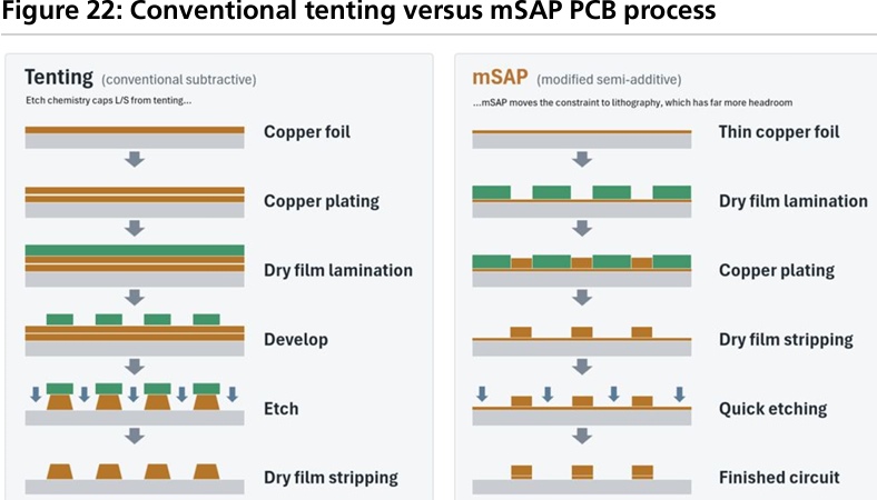
The subtractive process is the standard HDI method. Copper foil is laminated to the dielectric, plated up to thickness, covered with a resist pattern, and everything unwanted is etched away. It is reliable and economical for line and space of about 40 microns and above.
The modified semi-additive process starts with a very thin copper layer. Copper is plated up through openings in a resist, the resist is stripped, and a short etch removes the thin starting layer. It handles line and space of around 25 microns in volume production.
The semi-additive process with build-up film is the substrate route. It uses ABF film and reaches 20 microns and below, often around 15 microns or finer.
In short, subtractive serves mainstream HDI, mSAP serves the middle ground, and SAP with ABF serves IC substrates. For many projects, the middle option is the sweet spot, because it brings fine-line capability to a shop that already builds PCBs.
How the Process Works, Step by Step
The flow looks like normal HDI with a few important changes, and walking through it shows where cost and yield risk come from. In the PCB mSAP process, the circuit is grown by plating, not carved by etching.
First, the material. The laminate carries an ultra-thin copper foil, around 3 microns thick. This is the seed copper, the base from which the circuit grows.
Second, drilling. Density depends on blind microvias, and the holes are small, typically around 60 microns. CO2 laser drilling is the usual method, and registration between the hole and its pad leaves very little margin.
Third, making the via walls conductive. After drilling, the board goes through desmear, electroless copper and a flash copper step. The thin foil, the electroless layer and the flash copper together form a seed layer of roughly 3 to 4 microns.
Fourth, imaging. Dry film is laminated, exposed with a high-precision direct imaging system and developed. Alignment and resolution here largely decide the quality of the finished line.
Fifth, pattern plating. Copper builds up only inside the resist openings. Because the line is grown, the sidewalls are straighter and the geometry is more consistent.
Sixth, strip and flash etch. After the resist is removed, a brief etch clears the exposed seed layer between traces. Since that layer is only about 3 microns, the etch is short and the traces lose very little. In a subtractive flow, copper plated to around 20 microns must be etched through its full depth. That difference is the whole reason fine lines become possible.
The sequence repeats for each build-up layer. Solder mask, surface finish and electrical test follow as on any other board.
Copper Foil: The Material That Decides Everything
If one material makes or breaks mSAP, it is the foil. It must meet two requirements at once.
It must be ultra-thin, about 3 microns, so the final etch is short and undercut stays low. And it must have low roughness, around 1 micron or a little above. Standard HDI foil has a rough side well over 4 microns, which grips the resin but works against fine lines, because copper can stay trapped in the valleys after etching and cause shorts. A smoother surface also reduces loss at high speed, since current travels close to the surface at high frequency.
Foil suppliers sell several grades. Standard foil is used in ordinary HDI. Very low profile foil, often called HVLP, is used in high-speed HDI, and the best grades go below 0.5 microns of roughness. Foil made for mSAP is a separate family. An entry grade suits 800G products, a middle grade with roughness around 1.3 microns is the mainstream choice for 1.6T optical modules, and a higher grade near 0.9 microns serves the most demanding designs.
One detail catches many buyers: a lot of 1.6T boards are hybrids that combine conventional HDI layers with fine-line layers. The HDI layers still need HVLP foil to keep high-speed signals clean, while the fine-line layers use the mSAP grade. Always specify both.
Raw materials have also become more expensive. Core and prepreg prices have risen sharply this year, and high-speed foil has gone up as well, which is why quotation validity periods are shorter than they used to be.
Why Not Every Factory Can Do It
You cannot switch a normal HDI line to this process by changing a recipe. It needs equipment that standard lines do not have, plus upgrades to equipment they already own.
Vertical continuous plating gives even copper deposition on a thin seed layer across a large panel. Uniformity matters because plated height affects both resistance and impedance on a 25 micron line.
High-precision direct imaging is the most critical piece. On a 1.6T optical module board, the DSP uses a BGA with roughly 130 micron pitch. Pads are about 110 microns across, leaving a gap of only about 20 microns. The imaging system must place resist openings accurately enough for that geometry to be repeatable.
CO2 laser drilling machines built for small holes and tight registration are needed for 60 micron blind vias. Vertical developing equipment gives uniform development before plating. Inspection must keep up too, since automated optical inspection that works well at 50 microns may miss defects at 25.
Equipment is also what limits how quickly capacity can grow. High-end machines often take a year or more to arrive, and expedited orders can still take six to eight months. Installation and tuning add about two months, followed by equipment qualification and customer qualification. That is why qualified capacity is tight and why early planning matters.
Where mSAP Boards Are Used
Premium smartphones were the first large users. Flagship mainboards, typically ten or twelve layers with around 30 micron lines, adopted the technology early because boards kept shrinking while chips kept getting denser.
The growth story today is in AI-related products. Optical modules are the biggest driver. The move from 800G to 1.6T brings a DSP package and tight pitch that standard HDI cannot route. ABF substrates would solve the density problem, but they are costly and capacity is limited, so the PCB route is attractive. Many of these boards are 14 layer hybrids combining HDI and fine-line layers.
Smart glasses and wearables are small, power-limited and full of sensors, which favors fine lines. Volumes are still modest compared with optical modules, but the direction is clear.
AI servers are the next candidate. Main processors still connect through ABF carriers, but as compute grows, parts of the board near the carrier run short of routing room. When die pitch reaches about 130 microns and traces must be under 30 microns, standard HDI falls short. Broad adoption has not happened yet, but some regions of next-generation server boards are expected to move this way.
A quick test for your own design: check the BGA pitch, check the escape routing you need, and check whether the lines are narrower than about 40 microns. If so, talk to a fine-line supplier early.
Phone Boards and Optical Module Boards Are Not the Same
Both are made with mSAP, but the difficulty differs. A typical flagship phone board runs 30 micron lines and spaces, layer-to-layer alignment of about 35 microns and a processing tolerance near plus or minus 100 microns.
A 1.6T optical module board is tougher on every count. Lines and spaces drop to 25 microns, alignment tightens to 20 to 25 microns, and tolerance narrows to about plus or minus 50 microns. Nickel palladium gold is a common finish, which raises requirements for pad cleanliness, flatness, gold coverage and resistance to sodium ion migration. So do not assume that phone board experience equals optical module experience. Ask for process data at your level of difficulty.
mSAP Compared with ABF Substrates
Because both use plating to form lines, people often confuse them. Three differences matter in practice.
Material: ABF substrates use build-up film with no glass cloth, while mSAP boards still use prepreg with glass cloth. Seed layer: in substrates it is electroless copper under 1 micron, while mSAP uses foil plus electroless plus flash copper, around 3 to 4 microns, which means a slightly longer final etch and a higher practical limit on line width. Line and space: substrates can reach 2 to 3 microns, while mSAP works at the 10 micron class and above, with volume products today around 25.
That gap is precisely why mSAP is useful. It sits between HDI and substrates, with a cost and supply chain that suit products which do not need substrate-level geometry.
Lead Time and Pricing
Demand from optical modules has grown faster than qualified capacity, and large fabricators must protect commitments to existing customers first. Many observers expect supply to stay tight through 2026 and into 2027, with relief possible around the second quarter of 2027 as new lines complete qualification.
On price, materials have gone up, and when supply is short, quick-turn orders and samples often carry a premium. The sensible response is to confirm specifications and reserve capacity early, not to shop on unit price at the last moment.
What You Need to Send for an Accurate Quote
Gerber files or ODB++ data, layer count and stack-up (including any hybrid structure), target line width and spacing, minimum blind via and pad size, preferred laminate and foil grade, surface finish, impedance requirements, board size and quantity, and any special test or reliability requirements.
If you are unsure about any item, send what you have. An engineering review can often suggest practical changes, such as limiting fine lines to the escape area under the chip, which reduces cost without hurting performance.
Design Tips That Save Time
Share the stack-up early, especially if it is a hybrid, because many problems come from discovering late that a material chosen for one area conflicts with the process needed for another. Use fine lines only where needed, since routing everything at minimum geometry raises cost and risk. Design pads and via landings with realistic margins, because a design that assumes better than a plus or minus 50 micron tolerance will lose yield. Plan test access from the start, and discuss impedance targets together with geometry, since thin dielectrics and narrow lines make impedance sensitive to small plating variations.
Frequently Asked Questions
What is the minimum line width for the PCB mSAP process? Volume production typically runs at around 25 microns line and space. Finer geometries are possible in development work, but they depend on foil, imaging equipment and the design itself.
Is mSAP the same as HDI? No. HDI usually refers to boards built with a subtractive flow and laser microvias, suited to lines above about 40 microns. mSAP is a different line-forming method for finer lines.
Does mSAP always cost more? Per square meter, yes, because of the thinner foil, extra equipment and tighter process control. It can still be cheaper than an ABF substrate for the same function.
Can existing HDI designs be converted? Often yes, but the stack-up, foil, pad design and tolerances usually need review.
Start Your Project
If your next design includes tight-pitch BGAs, high-speed lanes or dense escape routing, send your files and requirements for a technical review. Share your target line and space, via size, stack-up and quantity, and you will get feedback and a quotation. A clear brief at the start saves weeks later, and the PCB mSAP process rewards buyers who ask good questions early.