Circuit Diagram and PCB Layout: Core Differences and Engineering Boundaries
2026-10-23
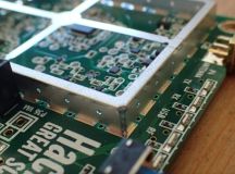
Circuit diagrams and PCB layout sit on different design layers. A schematic defines circuit topology, component parameters and electrical connectivity, generates netlists and passes ERC for logical validation. PCB layout implements physical placement and routing under netlist constraints, exports Gerber files and runs DRC to check geometry and manufacturability. Linked by netlists, schematics confirm theoretical function, while PCB layout governs real-world signal integrity, thermal performance and hardware reliability.
See details>